Hello. I use in my project ADC ADS1220. I initialize ADC settings only 1 time at program start. While the program is running, I switch the channels of the multiplexer and set gain. And I noticed that while the program is running, the data rate is reset. It is set to the default value. I can not say for sure whether all the ADC registers are reset, but this parameter is reset exactly. This happens irregularly. The program may work normally for several days, and then a register reset may occur, but a reset may occur after a few hours. Tell me, please, what could be the reason?
Power settings:
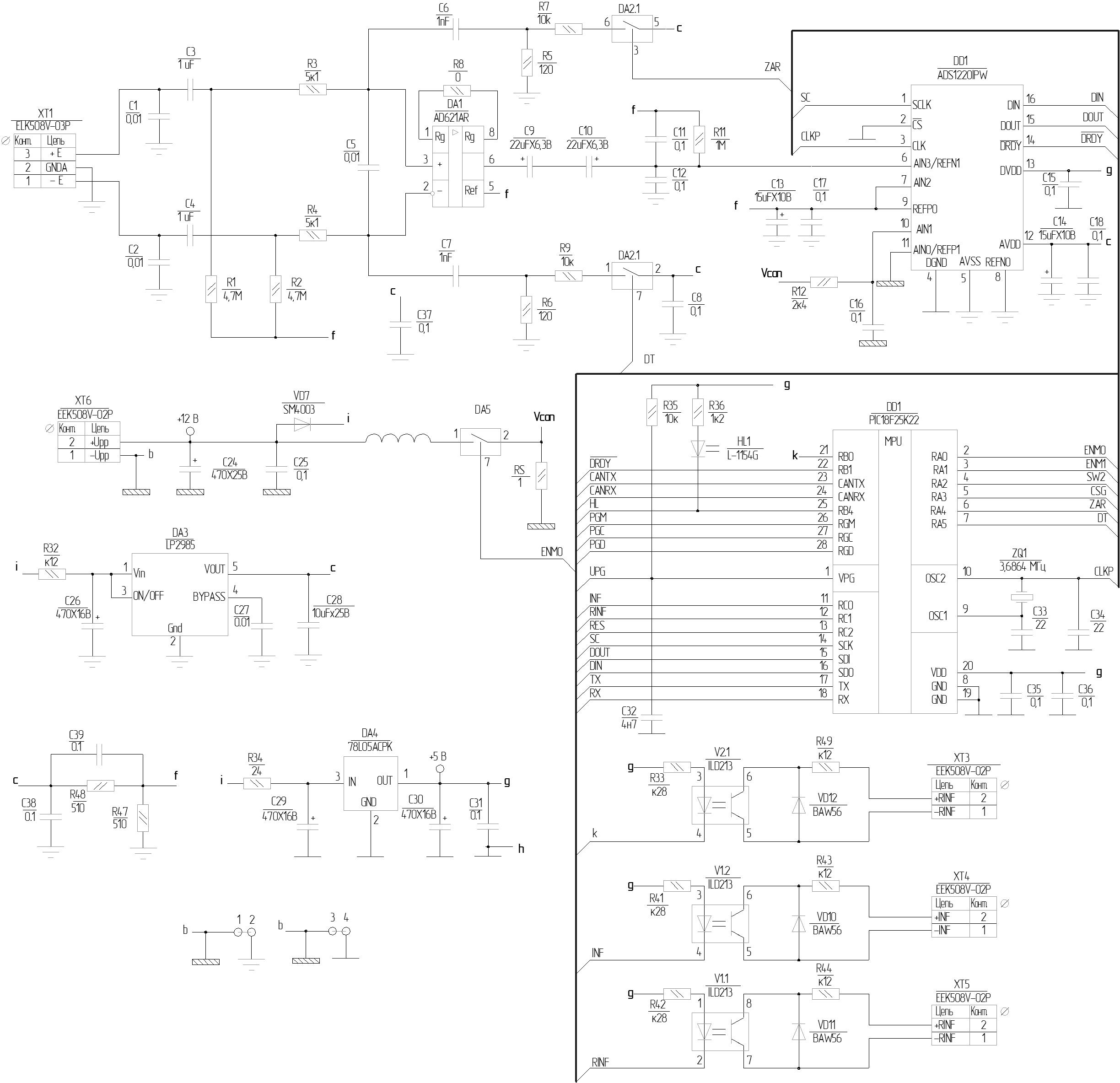
AVDD = 5V
DVDD = 5V
AVSS = GND
Ref = 2.5V
ADC initialization function:
void init_adc(void)
{
long in_adc = 0x0000A0E0;

//reset settings
SPI_Send_byte(0x07);

// Delay a minimum of 50 us + 32 * tclk
del_50();
Delay10TCYx(4);

wrreg(0, 4, in_adc); // starting from the Configuration Register 0, 4 bytes, value 0x0000A0E0

// start
SPI_Send_byte(0x08);
}
ADC settings at program start:
Input multiplexer configuration = AINP and AINN shorted to (AVDD + AVSS) / 2
Gain = 1
Normal mode
Single-shot mode
Data rate ~ 440 SPS (DR Bit Settings = 101)
Fosc = 3.686400 MHz
SCLC = Fosc/16
I use the following functions while the program is running (I select the channel and set the gain):
unsigned char KuU[8] = {0x00, 0x02, 0x04, 0x06, 0x08, 0x0A, 0x0C, 0x0E};

void set_u(void) {
	wrreg(0, 1, (0x70 | KuU[i]));
}

void set_uc(void) {
	wrreg(0, 1, (0xE0 | KuU[i]));
}

void set_ic(void) {
	wrreg(0, 1, (0xE0 | 0x02));
}

void set_i(void) {
	wrreg(0, 1, (0x60 | 0x02));
}