This thread has been locked.

If you have a related question, please click the "Ask a related question" button in the top right corner. The newly created question will be automatically linked to this question.

ADS1220: ADS1220 - question regarding common and differential mode filters for analog and reference inputs

Part Number: ADS1220
Hi Bob,
Thank you very much for your help and suggestions regarding troubleshooting my issues with obtaining reliable SPI communications between ADS1220 part and Raspberry Pi 3.
I completely agree with your comments regarding the advantages of using a single PCB with all the circuitry to reduce any inductance or capacitance caused by wires.
It makes sense that the 100uF caps I added act as reservoirs to supply power to the ADS1220 part when the wire inductance may act to choke the currents required
for operation. I will probably transition to a single board design after my initial testing and development phase is complete. The single board design should help reduce or eliminate the
voltage spikes that I have been seeing and perhaps with the single board design I won't need as large of caps on the ADS1220's digital and analog supplies.
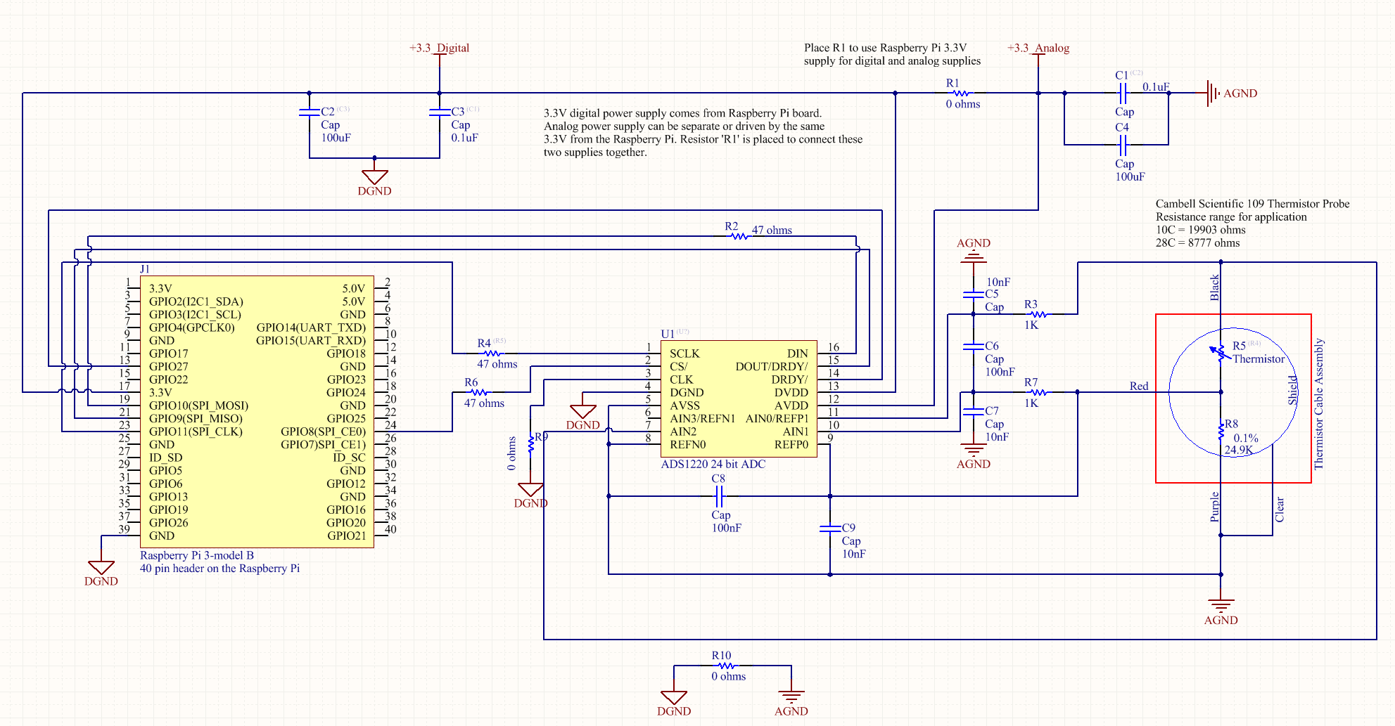
Below is an updated schematic showing the common and differential mode filter caps on the analog inputs as well as the voltage reference to the ADS1220.
Can you please tell me if this looks correct. I am not sure if I should also have series 1K resistances on the REFP0 and REFN0 pins.
Thank you again for your help and time.

-Sean

  • Hi Sean,

    You could add a resistor at the REFP input to help filter noise. Otherwise it looks pretty good.

    Best regards,
    Bob B
  • Thank you Bob. I will add a 1-2K resistor at the REFP input as you suggest to help filter noise.
    I appreciate your help with my project and usage of the ADS1220 part.
    -Sean

  • Hi Bob,

    I have been thinking about the resistor you suggested on the REFP input to help with the noise filtering. I am not sure if would matter if the resistor was placed between pin 9 (REFP) and the C8 & C9 common node OR if the resistor was placed between pin 9 and the R7 & red wire common node. The later would be more similar to the placement configuration of the other series 1K resistors and their respective caps for the AIN0 an AIN0 inputs. This would seem to form an RC low pass filter. But I wanted to get your input.
    thank you.

    -Sean
  • Hi Sean,

    The way to think this through is to consider the current path of the signal. For a low pass filter you want the signal to flow through the resistor before the signal sees the capacitor. So from the red wire the signal should go to the resistor and from the resistor to the cap/REF input on the ADS1220.

    Best regards,
    Bob B
  • Hi Bob,

    Thank you for the clarification regarding the placement of the resistor to achieve the proper low pass filter effect for the REFP0 input. Your explanation makes good sense and I will place the resistor between the red wire and cap C9 / REFP0 input node. 

    cheers,

    -Sean