This thread has been locked.

If you have a related question, please click the "Ask a related question" button in the top right corner. The newly created question will be automatically linked to this question.

ADS112C04: ads112c04 registers configuration problem

Part Number: ADS112C04

Hi!

Part A:

When I use ADS112C04, I met some problems.

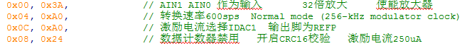
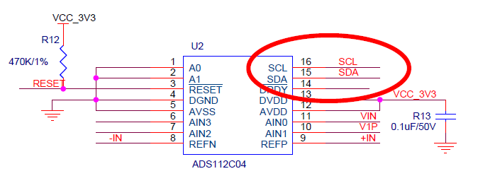
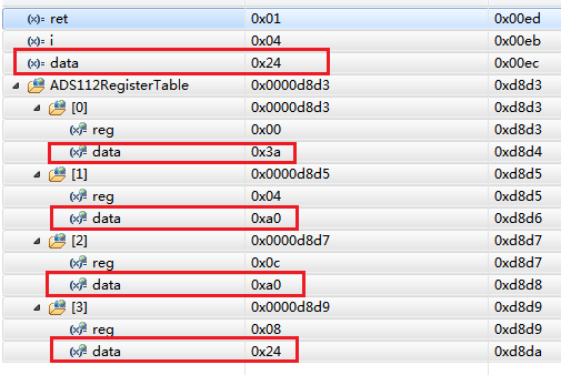
1 Configure 4 registers(Reg0~Reg3) through I2C

  write Reg0:0x3A // 

  write Reg1:0xA0 // 

 write Reg2:0xA0 // 

 write Reg3:0x24 // 

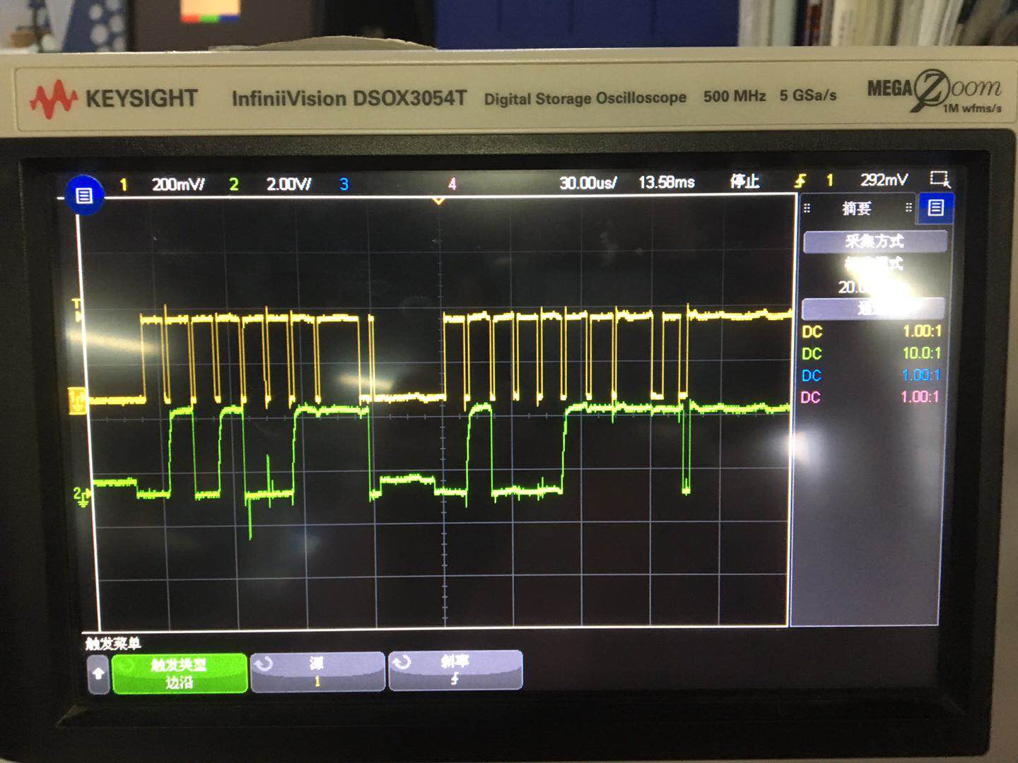
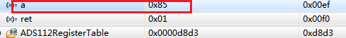
2 All 4 registers read and write normally in first time. then I read the register again, it's failure that the value is different with the first time and the AD samples is wrong.

you can see the figures as follow, please help to analyze.

Part B:

As described above. I have another problem. Do you have the recommended configuration? And is the configuration order required ?


BRs,

Barret 

  • Hi Barret,

    There is an issue with part A.  I will assume that the contents of 'reg' is the register position to be 'OR'ed to the WREG or RREG commands.  The values for register 2 and register should be changed so that register 2 is 0x08, and register 3 is 0x0C.  Currently 0x24 is being written to register 2 and 0x0A is being written to register 3.

    It would be helpful to see a schematic, some scope or logic analyzer shots of the communication, and the register settings read from the device that are incorrect.  It is possible that a transient is causing a reset of the device if the registers are at the default settings.

    Regarding part B, the registers can be written in any order.

    Best regards,

    Bob B

  • Hi Bob,

    We have configured reg WREG or RREG that RREG is 0x20|reg and WREG is 0x40|reg.

    Also, you can see our program. I will get the problem of yestoday if i run this.

    Highlight: why does the value of reg changes.

  • add the schematic

  • Hi Barret,

    What value of pull-up resistor are you using on the SCL and SDA lines?  What SCL clock speed are you using?  Can you share scope or logic analyzer shots of the communication for me to evaluate the response from the ADS112C04?  

    The RREG command requires a device address/write of the command, followed by a repeated start, followed the device address/read followed by the data (Figure 58 of the ADS112C04 datasheet).  Have you verified that you are getting the proper ACK?  What data are you receiving from the RREG command?

    As you are turning on the IDAC to REFP, what is connected to REFP (+IN) and REFN (-IN)?  What is connected to AIN1 (V1P) and AIN0 (VIN)?

    Best regards,

    Bob B

  • Hi!

    What value of pull-up resistor are you using on the SCL and SDA lines?  What SCL clock speed are you using?  Can you share scope or logic analyzer shots of the communication for me to evaluate the response from the ADS112C04?  

    I don't use pull-up resistor because the distance is so short. The scope shot as below


    As you are turning on the IDAC to REFP, what is connected to REFP (+IN) and REFN (-IN)?  What is connected to AIN1 (V1P) and AIN0 (VIN)?

    our schematic use the typical application of datasheet. You can see the connections as below:


  • Hi Barret,

    I2C is an open-drain system, which means that the output high from the slave device (in this case the ADS112C04) is based on the value of the source voltage with a pull-up to the source voltage.  It may be that your micro has a weak pull-up option on the pin, but usually this pull-up is too weak with respect to the required response time to overcome any line capacitance of the system.   I would suggest adding pull-up to the supply on the SDA line at the very least.  You can start by using a value of 4.7k Ohms to the supply.

    From the scope shot it appears that you are driving the SDA line from the micro and then going to high impedance when expecting the ADS112C04 to respond.  This would be ok from the micro perspective, but the ADS112C04 can only drive the SDA line low.  The ADS112C04 depends on the pull-up to set the SDA high line when responding. 

    A couple of other issues I see in the scope shot.  I do not see the correct START condition or the proper address being transmitted to the ADS112C04.  A0 and A1 are grounded  which means the I2C address is 100 0000 (0x40) for the ADS112C04 (Table 14 of the datasheet).  As you need to left shift the address by 1, the first byte transmitted would need to be 0x80 for a write and 0x81 for a read, as the least significant bit determines whether you are reading or writing to the I2C device.

    It appears based on the appearance of the scope shots that you are bit-banging the GPIO ports.  If this is true, try to adjust the clock timing so that the duty cycle of the clock (with respect to high time and low time) is closer to 50/50 instead of 90/10.  Regarding START and REPEATED START the SCL needs to be high then SDA goes from high to low followed by SCL going low.

    Best regards,

    Bob B