This thread has been locked.

If you have a related question, please click the "Ask a related question" button in the top right corner. The newly created question will be automatically linked to this question.

ADS1262: TDAC settling time

Part Number: ADS1262

Hello, 

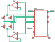
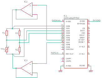
I intend to use internal TDAC of the ADS1262 which output I bring to AIN6, AIN7 and form there to unity gain buffer. 

What is settling time of the TDAC value? Can I see TDAC output on AIN6, AIN7 when Chop mode eneabled? 

Is there a way for TDAC to operate from internal 2.5V reference instead of the AVCC-AVSS ?

Thank you for your help

Jan

  • Hi Jan,

    The TDAC inside the ADS1262 is a resistor divider between the AVDD and AVSS supplies. Unfortunately, it must therefore always run off of the 5 supply.

    The settling time of the TDAC is going to depending on the voltage output (as the output impedance of the TDAC changes with output) as well any capacitive load it must charge. The output impedance of the TDAC ranges anywhere from about 3kOhms to 25kOhms.

    You should be able to measure the TDAC voltage with the ADC (chop ON or OFF). In the INPMUX register, you can connect directly to the TDAC outputs, whether or not you enable the TDAC outputs on AIN6/7.

    Please note that the internal TDAC is a coarse DAC, mainly intended to exercise the PGA + ADC across the full input range of the device. It is not a precision DAC with high accuracy specs. If you do intend to use it with other external circuits you'll probably want to buffer it.

  • Dear Chris,

    thank you for the answer. To describe my idea in detail please see attached schematics (filters ommited fro clarity)

    I need to measure temerature 20-30°C with highest possible resolution (microKelvin) My intention is to build bridge with 3 fixed resistors and one NTC theremistor. 

    To get rid of parasitic thermocouples I want to have AC excitation as suggested in http://www.ti.com/tool/TIPD188. I want to be able to excite the bridge with 

    different voltages to evaluate self-heating effect of the thermistor, too. I will set TDAC1 to 4V and TDAC2 to 1V perform a couple of measurements, then I reverse 

    polarity by changing TDAC1 to 1V and TDAC2 to 4V and perform another couple of measurements. I can use different TDAC levels to see how 

    changes the self-heating of the termistor. The corase setting of the voltage is ok for this. Settling time around 1ms would be fine. Do you thing this could work?

    But it may happen that I will want to test DC excitation only. In this case I will use Chop mode to cancel internal offsets of the ADC. 

    Will TDAC generate output voltages on the AIN6 and AIN7 in this case? My concern  is sentence on the page 53 of the ADS1262 manual "Note that chop mode

    must be disabled to test the ADC with the TDAC." Please clarify what happens with TDAC in chop mode.

    Thank you for your comments

    Jan

  • Wow, It seems my schematics is way too small. So bigger one..

  • Hi Jan,

    I'm sorry for the delayed response.

    I looked into the the rationale for the warning to not use CHOP with the TDAC, and found that this only applies when you use the MUX to connect directly to the TDAC (i.e setting the INPMUX register value to 0xEE).

    In your case, where you route the TDAC outputs trough AIN6/7, buffer this voltage, and then measure it back through different input pins, it is OK to use the CHOP mode to measure the bridge output voltage...and yes, the TDAC output voltages are connected to the AIN6 and AIN7 pins by setting the OUTP and OUTN bits in the TDACP & TDACN registers.


    I don't see any issues with using the TDAC in the way you've described, especially since this voltage is buffered and you're measuring the bridge ratiometrically, which makes the measurement less sensitive to the TDAC noise. If you do use AC excitation, then you'll want to make sure that the TDAC fully settles before you start the next ADC conversion after switching the excitation voltage polarity (this includes any additional RC filters on the bridge output or the reference inputs to the ADC).