This thread has been locked.

If you have a related question, please click the "Ask a related question" button in the top right corner. The newly created question will be automatically linked to this question.

TLV2556: Invalid data after 'short' power down of 3s

Part Number: TLV2556
Other Parts Discussed in Thread: OPA2376

Dear Team,

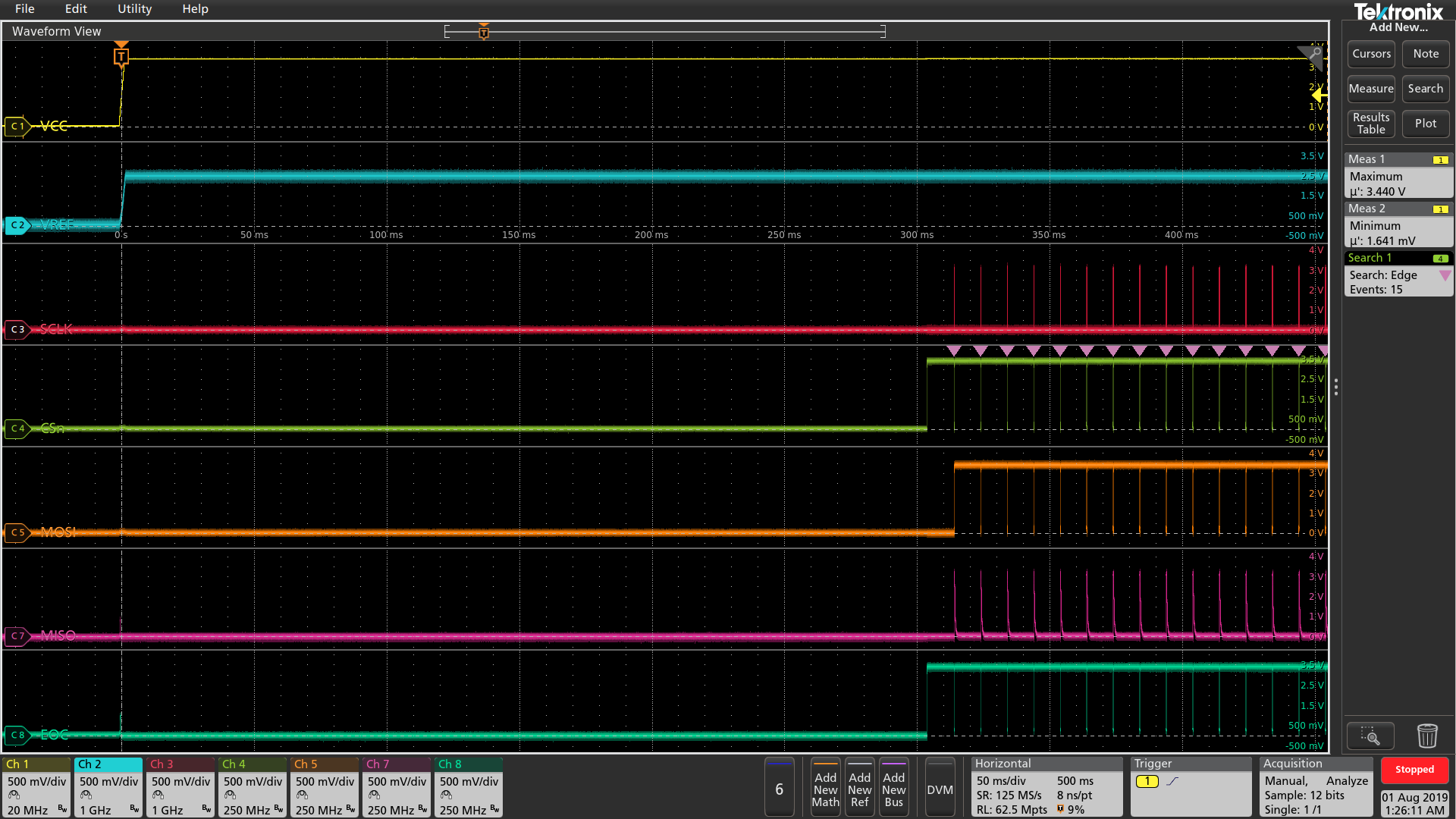
our customer reported a problem with the TLV2556.

In their system, they noticed that a power down cycle of 3s causes a wrong data sampling when the device starts up again. If the power-down is 4s, they do not see any problems. Reading out the test channels give correct values in both cases.

The system uses an external reference, and the ADC is using default values. The communication starts with writing CFGR1 to 0x0030 (select channel 0, 16-bit length, MSB first, unipolar binary).

Can you please advice what we need to check and do you have thoughts about the start-up / powering-up of the device that we could verify?

Thanks and best regards
Martin

(P.S.: We provided schematics and scope plots via e-mail to Art.)

  • Hi Martin,

    Can you please verify that the reference and associated analog input circuitry is also powering down completely during the 3 second versus 4 second power cycles?

  • Please, see the scope plot taken during the failing power cycling showing that both VCC and reference are powered-down withing first 0.8s. All ADC inputs are driven with an active filter with OPA2376 powered with the same 3V3 supply.

  • Hi Michal,

    I'm a little surprised by the way MISO is still looking like its trying to drive high there at the end of the sequence - and I've seen that on some of the plots that were sent over from Martin.  Gan you describe exactly what the corrupted data looks like at the receive side?  Are you perhaps missing an SCLK cycle along the way somewhere?

  • Hi Michal and Martin,

    Any feedback here?

  • Hello Tom,

    All the signals are measured at inputs of respective components. No active components are present in the signals, only series termination. Also, the test channels prove the communication is successful.

    Please, see the following batch of plots (all from one acquisition where the ADC returns invalid values). Please, excuse absence of labels in the zoomed plots, the order of waveforms is identical to the overview.

    1. Overview on power on

    2. 1st transaction, 1st word (full reference test channel [CH13]), correct data is received (0xFFF + padding):

    3. 1st transaction, 2nd word (CH0), incorrect data is received (0x005 + padding):

    4. 1st transaction, 4th word (CH2 - we know there is 1.8V at the input here), incorrect data is received (0x004 + padding):

    5. 1st transaction, 13th word (reference / 2), correct data is received (0x7FF + padding):

  • Hi Michael,

    I sent Martin a note suggesting we all get on a call to go over this.  Please let him know your availability.