This thread has been locked.

If you have a related question, please click the "Ask a related question" button in the top right corner. The newly created question will be automatically linked to this question.

ADS1260-Q1: Differential input

Part Number: ADS1260-Q1
Other Parts Discussed in Thread: ADS1261-Q1, ADS122C04

I have to read 4 strain gauge using 4 half bridges (2 half bridges with resistors, 2 half bridges with strain gauge), so I have to convert 2 differential voltage.

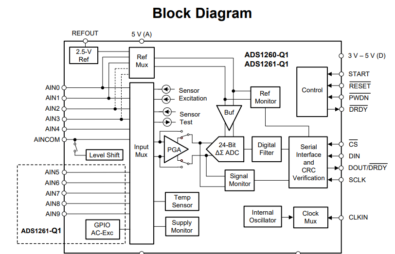
ADS1260-Q1 seems to have 3 differential inputs, how does it mean? because the chip has 5 single ended input. Can I use it? And if yes, can I use PGA on both the 2 differential inputs?

  • Hi Andrea,

    Welcome to the TI E2E Forums!

    The ADS1261-Q1 has 6 analog input spins, which allows for up to 3 fully-differential inputs, or 5 single-ended inputs when one pin is dedicated as a common reference. The ADS1261-Q1 measures all input voltages differentially, and the input voltage can be measured between any two analog input pins. NOTE: AINCOM is often used as a common reference in single-ended applications, but it is no difference from the other analog inputs and may be used for differential measurements as well.

    For bridge measurements, you typically want to measure each bridge ratiometrically. Meaning, the excitation voltage doubles as the ADC's reference voltage. When the bridge excitation voltage and the ADC reference voltage are the same, the input voltage and reference voltage are "ratiometric" (i.e. a change in reference voltage will result in the same relative change in the input voltage), which makes the measurement more immune to noise or drifts in the excitation voltage.

    If you can use a single excitation voltage for both bridges, and then provide that voltage to AIN0/AIN1 (to use as the ADC's reference voltage), then that leaves you with four analog inputs which can be used to measure the two differential voltages from each bridge.


  • Hi Chris,

    thank you for your reply. I will use the same voltage to supply both bridges (I think 2.5V or 3.3V) and I will connect it to for example AIN0.

    What do you suggest about capacitors at the input? 

  • Hi Andrea,

    Unless the bridge impedance is low (i.e. it will draw a large current) and susceptible to self-heating effects, I'd consider using the 5V analog supply for the ADC, as the bridge excitation voltage. The larger excitation voltage will increase the voltage output from the bridge and provide you with more dynamic range.

    For input filtering, I do recommend having small filtering capacitors. You might take a look at one of my previous posts where I give a bit more detail about anti-aliasing filters (here: https://e2e.ti.com/support/data-converters/f/73/p/826024/3069413#3069413).

    A differential capacitor somewhere on the order of 1-10 nF to help with noise filtering will likely be sufficient. Too large of a capacitor will take a long time to settle and larger leakage currents.

    Also, try to make the analog input filtering with the reference voltage filtering for optimal ratiometric noise cancellation.

  • Thank you Chris.

    Can you suggest me a similar delta sigma converter with I2C communication? The specification of the board is changed and I can't use SPI to communicate with the uC. The ADS122C04 seems good but the data rate is lower (2kSPS vs 40kSPS), I don't find something faster.

  • Hi Andrea,

    The ADS122C04 is probably the best option I can recommend with those requirements. We don't have any other I2C Delta-Sigma ADCs that are able to run at a faster data rate. The only faster I2C ADCs will be 12-bit SAR ADCs. With the extra overhead for I2C communication, you'll generally find that ADCs with an I2C interface are lower resolution and operate at much slower data rates than ADCs with SPI.

    For best resolution and noise performance, you'd likely want to run the delta-sigma ADC at a slower data rate to allow the digital filter to perform additional averaging for noise reduction. Therefore, lower data rates are usually fine in these types of applications.

    Is the faster data rate necessary for multiplexing between the two bridges quickly or for detecting step changes quickly?

  • Hi Chris,

    I'm developing a board prototype and at the moment high data rate are not fundamental, so I can use the ADS122C04.

    I convert the 2 bridges once a time so I will have maximum 1-kSPS each, but it should be enough for the application (force and torque sensor).

    As you suggested, I power the bridges with 5V: in the ADS122C04 datasheet I can see that REFP and REFN have been connected to 5V and AGND, is it a good choice a 100nF capacitor (Cdif2, page 59) between these pins?

    Best regards,

    Andrea

  • Hi Andrea,

    I think 100 nF is a reasonable value for a differential reference filtering capacitor.

    I would additionally recommend routing the REFP and REFN signals as traces back to the sensor (or to the header where the bridge sensor connects to your PCB), instead of dropping vias to the supply and ground planes near the ADC. By routing these signals as dedicated traces, you can keep some of the noise from these power planes out of the reference voltage, and you also get better matching between the excitation and reference voltages.

  • Hi Chris,

    finally I designed the board with the ADS122C04IRTER as you suggested.

    Thank you again,

    Andrea

  • Hi Andrea,

    You're welcome! I hope the ADS122C04 works out well for your design.

    Best regards,
    Chris