This thread has been locked.

If you have a related question, please click the "Ask a related question" button in the top right corner. The newly created question will be automatically linked to this question.

ADS1256: Data converters forum

Part Number: ADS1256
Other Parts Discussed in Thread: INA159, REF5025

Hi, 

I have a sensor with a voltage output of plus-minus 10 V. 

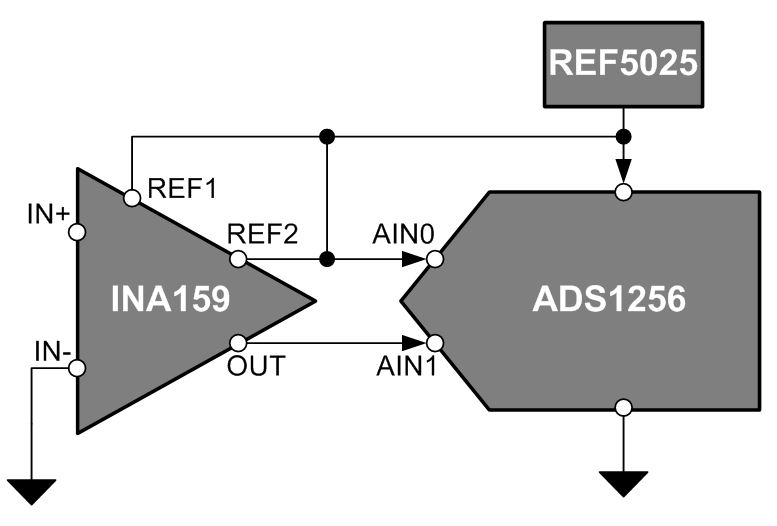
In order to use it I bought an INA 159 and an ADS1256.

The Ads is part of a raspberry pi hat, called waveshare ad/da precision board :

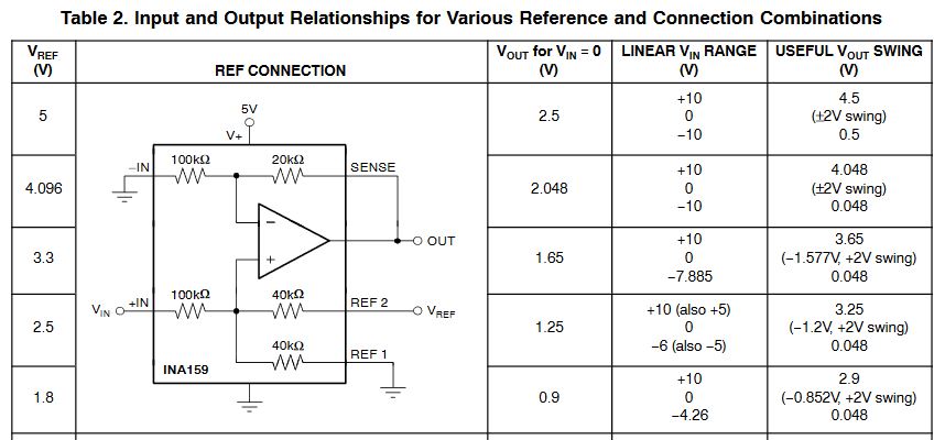
The setup works,  however I have a problem with the reference voltage for the INA. I put Ref 1 on ground, ref2 I connected with the VCC of the raspberry pi hat. This makes no sense, I guess, because this is just the voltage of the USB power. Actually, the adc gets its reference voltage from a LM285, which outputs 2.5 v on vrefP which goes in pin 4 of the ADS1256. 

Should i connect ref 2 to pin 4 of the Ads to use vrefP as reference for the INA? Should I connect ref 1 and 2 together in this case?

Is there any other way to get independent from the reference voltage?

Cheers 

Nils 

  • Hi Nils,

    The image below shows the INA159's output scheme given the connections you described (REF1 = GND, REF2 = VCC). I am not sure what VCC is on the waveshare board since this is not a TI product, but if it were 5V for example then the INA's output swing would be +/-2V, centered around 2.5V as shown.

    If you were to connect REF2 on the INA159 to VREFP on the ADS1256, this would give you an unbalanced swing of -1.2V to +2V, centered around 1.25V. It is really up to you to determine what output voltages you want to apply to the ADC. With the ADS1256's buffer disabled, the ADC can handle either of the scenarios I just described. If you have enabled the buffer, please be aware that the absolute input voltage the ADC can accept is AVDD-2V, which is likely somewhere around 3V.

    -Bryan

  • Hi,

    Thanks for the answer.

    My problem is, that I want to calculate the measurements converted by the INA 159 back to the, let's say original, voltages the sensor put out.

    Thus, I think I have to feed the INA 159 exactly with 5 V to know, how the actual measured voltages of the ADS1256 relate to the sensor. At the moment I feed the INA with the power supply voltage of the ad board, which is in my case 5.3 V from a USB power supply. Thus, the "zero" line of the INA is at 2.55 V and the maximum (+10v from the sensor) give me 4.55 V.

    Now, how do I avoid this shift. I had the idea to measure on a channel the reference voltage. However, that doesn't work with the ads1256, because it can't digits voltage above 5 V, right?

    So my question is, can I make a setup with the INA and ads IC where I correct for errors/shifts in the reference voltages.

    Cheers

    Nils

  • Hi Nils,

    If your system was similar to the drawing below, then the INA159's output swing would be 0.5 V to 4.5 V given an input voltage on IN+ of -10 V to +10 V. This is shown in the bottom half of Table 2 in the INA159's datasheet. I referenced Table 2 in my previous post, but only included the top half of the table. Note that the block diagram below does not include all inputs, supplies, etc., and is used for illustrative purposes only.

    If IN+ = 10V, then OUT = 4.5 V and REF2 = 2.5 V using REF5025. So the ADC sees AIN0 = 2.5 V and AIN1 = 4.5V. If you were measuring from AIN0 to AIN1, then the ADC would see a differential voltage of 2.5 V - 4.5 V = -2 V.

    Similarly, if IN+ = -10 V, then OUT = AIN1 = 0.5 V and REF2 = AIN0 = 2.5 V. So, AIN0 - AIN1 = 2.5 V - 0.5 V = 2 V.

    Combining these two results, the ADC sees a differential input voltage of ±2 V. Table 16 on page 23 in the ADS1256's datasheet shows how the ADC's output code scales with input signal. As shown in this table and in the Electrical Characteristics section (pg. 3), the ADS1256's full scale range = ±2*VREF / PGA. Assuming PGA = 1 and VREF = 2.5 V, then your max code of 8,388,607 corresponds to an ADC input voltage of 5V, while your minimum code of -8,388,608 corresponds to an ADC input voltage of -5V. In your system, you are only using 40% of the ADC's full scale range, so a 2 V ADC input yields an output of ~3,355,442 and corresponds to IN+ = 10V, while a -2 V ADC input yields an output code of ~-3,355,443 and corresponds to IN+ = -10 V. Note that these are ideal codes, and do not factor in effects of noise, INL, offset, gain error, etc.

    It would be possible then to use a gain of 2 on the ADS1256 to double your available code range. So I do not believe you need a 5 V VREF, and I would instead suggest using VREF = 2.5 V per the calculations shown here.

    -Bryan

  • Hey abrian,

    Thanks a lot, that almost solved my problem. Is it correct, that a PGA of 1 is OK, when the reference voltage is 2.5 V at the INA? You said, when I'm using 5Vref I do not use the full range of the ADS, didn't you?

    Last question about the INA: the datasheet says it's good layout practice putting a bypass capacitor on the supply pins. Can you make a sketch how best practice would look like to connect the INA to the ads and to the power supply? There is also a RC filter suggested in the output of the INA to the ADS, right?

    Best,

    Nils

  • Hi Nils,

    Yes you can use a gain of 1 or a gain of 2 given the inputs I mentioned in my last email. The gain of 2 will use more of your allowable code range however, but that choice is up to you. This was using a 2.5V reference, not a 5 V reference.

    The recommended connections for the ADS1256 are shown in Figure 25 in the ADS1256 datasheet. Please reach out to the amplifier team via E2E for recommendations on the INA159, since they will have the best knowledge on that subject.

    You will need an anti-aliasing filter between the INA and ADS1256. Figure 25 shows possible values for the resistor components. The intent of the filter is to reject multiples of the modulator frequency, fMOD, which is just fCLKIN. This is nominally 7.68 MHz for the ADS1256. A cutoff that is 10x lower than fMOD will provide 20dB of rejection, while a cutoff that is 100x lower provides 40 dB of rejection. The tradeoff is the settling time of the filter can't be too small depending on how fast you want to sample your input, otherwise your inputs might not settle in time. Just something else to consider.

    Once you have put together a schematic, we can quickly review it for you.

    -Bryan

  • Also, to be clear, the ADS1256 cannot accept a differential 5V reference (or anything >2.6V), if that was the intention