This thread has been locked.

If you have a related question, please click the "Ask a related question" button in the top right corner. The newly created question will be automatically linked to this question.

8-bit Multiplying DAC TLC7524

Other Parts Discussed in Thread: TLC7524, LM339

Hi Guys,

I am a student working in a testing class. I am trying to test one Digital to Analog converter TLC7524 in a testing project. I downloaded the datasheet and I am trying to understand the datasheet. I am confused about several questions:

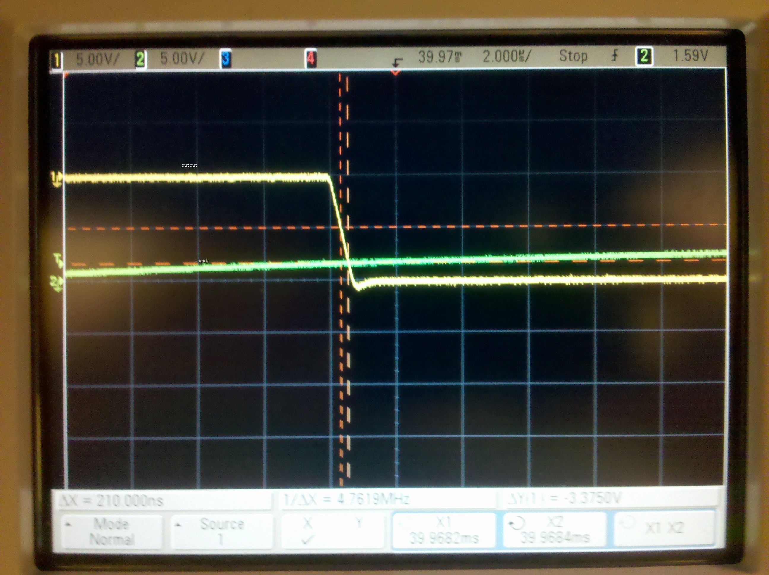
1. "electrical characteristics over recommended over recommended operating free-air temperature range, Vref=+-10V, OUT1 and OUT2 at GND". Does that mean that OUT1 and OUT2 need to be grounded when I test the parameters?

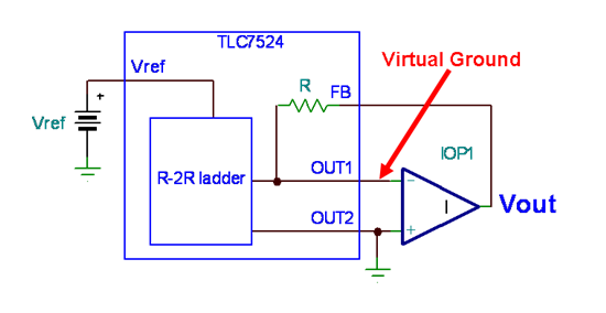
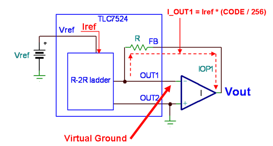
2.I don't understand how OUT1 and OUT2 work. It is said that the binary-weighted currents are switched between the OUT1 and OUT2. Does it mean that the analog output will appear at OUT1 or OUT2 depending on different digital input codes? But in the unipolar operation and bipolar operation diagrams, the OUT2 is always grounded.

3.What is RFB exactly used for? In principles of operation, RFB is connected to a resistor Rb and then connected to the output of an amplifier. Between Rb and OUT1, there is a capacitor. It is said that the Rb and C are only used under some conditions. Does that mean if the application is not in some condition the Rb and C don't need to be used and the pin RFB is just connected to the OUT1 and the output of the amplifier?

4. One amplifier is used to generate the output. Is it necessary? If it is necessary, what type of the amplifier is appropriately to be used? We don't use this device in a specific application. We just want to get some reasonable analog outputs from this DAC. Could you give us some recommendation?

5. This DAC consists an inverted R-2R ladder. So the analog output should be inverted, such as if the Vref is positive, the analog out should be negative. Is it correct? But in the unipolar operation, there is an inverted amplifier connection in the output termination. So the final output of this application should be positive, is it right? However, in Table 1, the analog output is negative.

6. In Page 4 of the datasheet, Note1 says Cext = 13pF. The Cext here is the capacitor in the diagrams in Page 7?

By the way, I am also looking for a IBIS model of this device. Is there anyone who has or knows where I can get it or a IBIS model which is similar to this part? Could you please answer those questions? I will greatly appreciate it.

Thanks and have a good day,

Yihong

  • Hello Yihong,

    1.-
    The part’s specs are characterized with OUT2 grounded and an opamp driving OUT1 to zero volts. Thus, OUT1 is not connected to ground, but it is made a virtual ground by the opamp like this:

     
    2.-
    Vref provides a total current Iref, and this current is sent to OUT1 or OUT2 depending of the digital code. From part to part, this current can be between Vref/20kΩ to Vref/5kΩ.
    In summary, the digital code controls that percentage of current that is sent to OUT1 as expressed in the following formula:

    I_OUT1 = Iref * (CODE / 256)

    For example, for code 0xFF, 99.6% of Iref is sent to OUT1 and 0.4% is sent to OUT2. Then, in order to keep OUT1 voltage equal to zero, the opamp output takes this current. When this current passes by the internal resistor in FB a voltage equal to –Vref*99.6% is developed at the output of the opamp.

    For code 0x7F, 50% of Iref is sent to OUT1 and 50% is sent to OUT2. Then, the opamp only takes half of Iref from OUT1. This develops an output voltage of –Vref/2.

    For code 0x00, 0% of Iref is sent to OUT1 and 100% is sent to OUT2. Then, the opamp doesn’t need to take any current from OUT1. This makes the voltage developed to be very close to zero.  

    3.-
    The optional resistor RB and RA are used to amplify the voltage. If amplification isn’t required, connect the output of the opamp to the FB pin and the reference voltage to the REF pin. The feedback capacitor, C, is only required if the output voltage is changed very fast and/or if the opamp selected requires it.

    4.-
    An opamp is indeed required to use this DAC. The selection of the opamp depends on the speed the output is changed. In general, if the output is not changed very fast any dual supply opamp should work fine.

    5.-
    Since the DAC needs to convert current to voltage, the opamp configuration should be inverting, so a negative reference must be used to produce a positive voltage. Another simple alternative to a negative reference is using a second opamp to invert the negative voltage produced when using a positive reference.

    6.-
    Yes, Cext is equivalent to the capacitor in page 7.

    This part doesn’t have an IBIS model, and I couldn’t find any other model similar to the TLC7524. However, it may be possible to use a low speed 8bit memory IBIS. 

    Nevertheless, all IBIS models are located in each product folder or in this link:
    http://focus.ti.com/adc/docs/midlevel.tsp?contentId=23670
           

  • Thanks a lot, Rafael. I greatly appreciate it.

    I have one more question. This DAC also has the voltage mode operation. In voltage mode, a fixed voltage is placed on the current output terminal. The analog output voltage is then available at the reference voltage terminal. So is it correct that we don't need to use the opamp if we use the voltage mode operation? In this case, how do we connect the RFB pin, grounded or no connection?

    Thanks,

    Yihong

  • Hi Yihong,

    Generally when designing with converters I try to avoid leaving any pins floating. I have seen some interesting effects with floating pins causing incorrect conversions. For that reason, I recommend that you connect the RFB pin to the current output terminal. This way RFB and the IOUT pin are both connected to your fixed voltage, essentially shorting out the internal RFB resistor.

    Using voltage mode will give you an output voltage coming from your reference pin. You will probably want to add an external buffer amplifier after the DAC in order to isolate your DAC from the R2R resistor string. Otherwise, your output load will have an effect on the voltage division that occurs in the resistor string. If you are looking to use a voltage output DAC, why don't you use one of the voltage output DACs we offer in out large catalog. These are probably going to perform much better and usually include a build in op amp to isolate the DAC from your load.

    Regards,

    Tony Calabria

  • Hi Tony,

    Thanks so much for your answering. I am using this device as the DUT for a testing project. I was trying to figure out how to use the voltage mode. That's why I asked how to get the voltage mode working that time.

    I have another question is about the test condition for the settling time and the propagation delay. I know I need to use the load resister and the load capacitor. I am not sure where these two components are connected to. At the opamp's output?

    Thanks and have a good day,

    Yihong

  • Hi Yihong Yang,

    The settling time test is done using the DAC in the normal configuration using an op amp at the output to create an output voltage. We generally like to simulate an output load on the op amp / DAC for the settling time test to give you a behavior to expect. In our newer DACs, we like to include a resistor and capacitor in parallel with the output. However, for this DAC I believe we just used a resistor to simulate the output load and the Cext in the compensation capacitor shown in Figure 3.


    Regards,

    Tony Calabria

  • Hi Tony,

    Thanks a lot for your reply. I greatly appreciate it. 

    I have one more question about the model of this part. I could not find a IBIS model or spice model of this device. But I need to do some signal integrated simulation. Rafael mentioned that I can use a low speed 8bit memory IBIS model. Can you give me more information about what kind of low speed 8bit memory IBIS model I can use? The setting time is 100ns Max. Does that mean this DAC has 10Meg sample per second?

    Thanks,

    Yihong Yang

  • Hi Yihong Yang,

    The IBIS model will help simulate the analog characteristics of the digital I/O pins across time and temperature. However, we do not have an IBIS model specifically for this part and there are no plans to develop a future IBIS model (the part is very old). If you are not concerned about simulating the part across temperature, you may be able to get by with simulating the pin capacitance as about 10 - 20pF to see how it effects your system. I am not sure what the actual pin capacitance is, it may be larger than 20pF. I am not sure what Rafael was explaining about a memory IBIS, I will let him step in to explain further. My recommendation is to use a capacitor to simulate the effect of the line.

    The TLC7524 does not have an update rate spec, but it does have a settling time and propagation delay spec. Because of the 80ns propagation delay, the update rate is going to be less than 10 Meg samples per second. I would expect the max update rate to be closer to 5 MSPS.

    Regards,

    Tony Calabria

  • Hi Tony,

    Thanks a lot for your help. 

    Now I have one more question here about TLC7524. To do the settling time test and propagation delay test, I connected the output to the load 100ohm (which is from the data sheet). Once I connected the road, I ramped the digital codes from 00000000 to 11111111 and measured the output voltage in both uni-polar and bi-polar modes. The full scale for the uni-polar is from 0v to -2.19v and for the bi-polar is from -2.6v to 3.2v. Without the road, the full scale for the uni-polar is from 0v to -10(255/256)v and for the bi-polar is from -10 to 10(127/128)v. 

    I could not understand it. Could you please explain it to me?

    Thanks,

    Yihong

  • Hi Yihong, 

    Do you have an IV output amplifier used to isolate the DAC's R-2R internal resistor string from the output load? If not, you are creating a voltage divider between with the DAC's internal resistor string and the output resistor.

    If you do have an output amplifier, look into the drive capability of that amplifier, it may be that the amplifier is unable to drive enough current to drive a 100 ohm load. Try increasing your load resistance to see if your output amplifier is having trouble driving 100 ohms.

    Regards,

    Tony Calabria

  • Hi Tony,

    I increased the load resistance to 2Kohms. The measured output voltage looks right. So I think my output amplifier is have trouble driving 100ohms.

    By the way, if we still use the same output amplifier but larger load to do the propagation delay test and settle time test, will the test results be in the specification range in the datasheet? Just for testing purpose.

    Thanks,

    Yihong

  • Hi Yihong,

    It depends on how you are looking at propagation delay. By definition it is the point from when the DACs shift register is updated to when the output has slewed 10%. If you are holding to that definition, then you can probably get a good idea of the propagation delay of the DAC. As for settling time, that is going to be more dependent on your output amplifier characteristics. The slew rate and small signal settling are two important factors which may be effected on what size load you decide on at your output.

    Regards,

    Tony Calabria

  • Hi,tony

    I'm working on a project about the driver of stepper motor.

    I use also the TLC7524, and i connected the circuit as what Rafael proposed, my Vdd is 5V,Vref 5V.

    But the maximum of the output is 4.4V, it can never arriver at 5V.

    I don't know why. and the wave is not correct.

    can you give me some suggestions? 

    thank you very much

  • Hi Ma,

    Did you end up putting an amplifier at the output for your MDAC to create a voltage? If so, then I would look into the specs of your output amplifier. What are you using for your IV output amplifier and I will take a look at the specs?

    -Tony


  • TONY,

    I used LM339 as amplifier.

    when i didn't connect the amplifier, the wave seems a little better. once i connect the amplifier, the output becomes very very small(10-20 mV).

    The Vcc of the amplifier is 5V too.

    In my waveform, what i wanted is that it should be between 0V and 5V.

    The conversion between 0-2.5V seems to be what i wanted. but the conversion between 2.5-5V can't be realized, when the output reaches 4.4V,it stops.


    I'm blocked here for about 1 week. I tried every possible reason,but i found nothing.


    thanks a lot for your reply.


  • from the photo,we begin from 0.

    i input the signal of a sine-wave,the first step is ok,the second ok,but the third one ,it should be much higher, we can see the difference between the 2nd and 3rd step is just 0.4V. Finally the 4th step,it should arrive at 5V.but it stops at 4.4V.

  • In this photo, i changed the number of steps from 4 steps to 16 steps.

    the wave became so confused. 


  • Hi Ma,

    It could be that you are saturating your output amplifier. Does the output behave correctly and step up as you would expect until you reach ~4.4V? At 4.4V, the output remains clipped at 4.4V as you continue to increase the codes. What are your power rails that the amplifier is powered off of?

    -Tony


  • Hi, Tony,

    I've tried but i'm afraid the problem is not here.

    i've tested in two conditions: with amplifier and without amplifier.


    When I didn't connect the amplifier, I could see the wave from 0-4.4V. If I augment the VDD to 7V or larger, the output become smaller than 4V. If I reduce VDD to 2V, the output become even much more smaller. 

    For example ,i give the Vref 5V,VDD 5V.  At the output from 0-2.5, it seems perfect. But the wave from 2.5-4.4, it's not what i want. I expect that i can find the output ranges from 0-5V, but not 0-4.4.


    When I connect the amplifier with VDD 10V, at the output I can find a signal very very small at about 30 mV. It seems there's somthing strange at the source. I don't know where it  is.


    thanks a lot for your suggestions.

    I'll try to find out somewhere else fault.

    Have a nice dream. Good night.

    MA   ^0^

  • 你好,

    很抱歉打扰你,我用这个DA转换器的问题很着急,不知道你能不能给我你的电话号码,我有几个问题想详细问一下。

    如果不方便的话,告诉我邮箱也可以。


    非常感谢

  • Hi Ma,

    If you can post your email I will contact you directly and we can take this into more detail.


    Regards,

    Tony

  • Hi Tony,

    Thanks a lot for your answers. That helps a lot. 

    Now I have one more question about the supply current : quiescent current and standby current. From the datasheet, I can see their test conditions are different. But I don't know exactly what are the definitions of these two currents. I setup the test conditions for DB pins for testing these two currents. But I could not get the current value in the range in the datasheet. Do I need to connect the CS/ and WR/ to the VDD when I do those tests?

    Thanks and have a good day,

    Yihong

  • Hi Yihong,

    Can you post a schematic of your setup? What current readings are you getting? Standby current is recorded when you are not communicating with the DAC. In this case, you would keep /CS high and /WR high to get an idea of the standby current. Quiescent current would be taken when /CS and /WR are both low indicating the DACs communication is active. 

    Regards,

    Tony

  • Yihong,

    After reading my reply, I realize it may not be the most detailed response. The quiescent current is going to occur at the threshold transition points which are when DB0-DB7 are at VIH or VIL max. At these points, the CMOS transistors will both be on for a brief period causing current to flow through. For the data sheet test, we use a static voltage to test for the quiescent current at those thresholds. Outside of the those thresholds, if DB0-DB7 are set high or low, you should be seeing the standby current.

    As for the parallel bus being enabled or disabled - my answer was assuming that the internal ''switch'' that disables the parallel bus is prior to the CMOS switches used to set the VIH and VIL limits. If internally the bus is disabled post-CMOS switch, then your may see the quiescent current even while the /CS is high. I understand this may be confusing so feel free to ask any questions that you would think would help clear this up.

    Regards,

    Tony

  • Hi Tony,

    Thanks a lot for your reply. I think I can understand you answer. We did the test setup again and got the reasonable test results.

    Now we have problem about the propagation delay and settle time test. The test setup is shown in the following picture. To do the test, all the DB pins are connected together to one functional generator, which is used to generate 1k Hz square wave. The low level is 0 V and the high level is 5 V. We used the oscilloscope to get the waveforms of the input and output. Here, we used 100 ohms resistor as the load at the output. But we could not get the full scare output voltage as I mentioned it to you before here and you suggested us to increase the load resistance. Then we used a 2K ohms resistor as the load and then we can get the full scare output voltage. Then we used the 2k ohms resistor to do the propagation delay and settle time tests.

    The definition of the propagation delay in the datasheet is from the digital input to 90% of the final analog output current. Instead of measuring the output current here, we used 90% of the final analog output voltage to get the delay time, which is from the input turned on to the 90% of the output voltage. The delay time we got here is about 8us which is much larger than what is said in the datasheet. If we used the definition of 50% to 50%, the 50% of the input is behind the 50% of the output voltage. I could not understand why this happened. 

    We used the same setup to measure the settle time, which is about 1.2us, much larger than the datasheet. 

    One more question about the diode protection on this chip. When we pull about 1mA current out from the pin, we can measure about 0.65V at the pin to the ground, which means there is a diode protection from the pin to the ground. But when we force about 1mA current into the pin, we got about 3V at the pin to the VDD (the Vdd is grounded). Does that mean there is no diode protection from the pin to the Vdd? Usually, there are diode protections from the pin to the ground and from the pin to the Vdd, right? 

    Thanks,

    Yihong


  • Hi Tony,

    Attached is the waveforms for the propagation delay and the settle time test. In the propagation delay waveform, the yellow one is the output and the green one is the input.

  • Hi Tony,

    I have one question about the Vih and Vil. In the datasheet, the minimum of the Vih is 2.4V and the maximum of the Vil is 0.8V. During the test, we connected all DB pins to ground except the pin which is being tested. We used one voltage supply connected to this pin and increase the voltage slowly from 0V to 5V and observe the output voltage changing (unipolar and bi-polar). We found then output voltage changed from 0 to 39mV (input: 00000000 to 00000001) when the input voltage for DB0 is about 1.4V to 1.5V. The output voltage changed from 39mV to 0V when the input voltage for DB0 is also about 1.4V to 1.5V. Here, the Vih is a little larger than the Vil, but not as same as the data in the datasheet. The same situation for the other DB pins. 

    I don't think the test setup is wrong here. But I could not understand it. Could you please explain it to me? 

    Thanks and have a good day,

    Yihong

  • Yihong,

    Regarding the settling time and propagation delay - These specs are heavily dependent on the characteristics of your output amplifier. You will need a very fast amplifier that can settle fast in order to fully characterize the DAC. It looks from your pictures that your op amp slew rate could be what is limiting those measurements.

    -Tony