This thread has been locked.

If you have a related question, please click the "Ask a related question" button in the top right corner. The newly created question will be automatically linked to this question.

DAC7568: Half output voltage after applying noise

Part Number: DAC7568

Dear Technical Support Team,

I'm testing DAC7568ICPW (C grade / Gain=2) with noise.

VOUT shows half voltage after applying noise(IEC61000) to power supply line.

Q1.)

Can you inform me  the cause of the DAC output being halved?

Q2.)

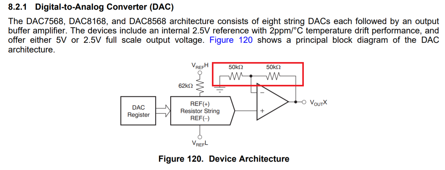
According to the datasheet , Vout formula is below. Gain is fixed by grade.

AVDD=5V and Internal VREF=2.5V then Gain=2 and output range is from 0 to AVDD

AVDD=5V and Internal VREF=2.5V , then Gain=1 and output range is from 0 to AVDD/2

And figure 120,I guess that both resistance 50kΩ of output amp set Gain=2 for C/D grades and  A/B grades has no  50kΩ resistance for buffer amp(Gain=1).

Is it correct?

3.)

Is it possible to change GAIN=2 to GAIN=1 by applying noise?

■Settings 

・Using internal reference 

・AVDD = 5V

■Conditions

・All  channel shows half of expected voltage. For example from 2V to 1V.

・Power line is below and applied noise to 24V.

 24V → 5V → AVDD 

・Noise (IEC61000) 

   Frequency from 90~130MHz  (Frequency increases 1.01 times every 1 second)

   Noise level 4V

   time: 60 sec

Best Regards,

ttd

  • Hi,

    Are you observing half voltage after applying noise? Before applying noise, DAC works as expected?

    Also in which power supply line, noise is injected? As I understand, you are generating 5V from 24V supply, noise is applied on 24V line?

    When you observed half voltage, what is the value you measured on Reference?

    Regarding your question on gain, it cannot be changed by applying noise. Its a fixed gain.

    You mentioned noise level is 4V, can you post the scope shots for the 5V supply when noise is applied? I am concerned here, because when you apply 4V noise on 5V supply, if it dips below the POR threshold, DAC can be reset with improper configurations.

    after applying noise, if you do a power supply reset, does the output comes back to normal?

    For C/D grade, its 2 and for others its set as 1 internally.

    Also output buffer is always set at gain 2 irrespective of the device grade, we have internally dividing the reference for A/B version so that total gain for DAC will be 1 in A/B version. 

    Regards,

    AK

  • Hi AK,

    >Are you observing half voltage after applying noise? Before applying noise, DAC works as expected?

    →Yes. When noise is applied to the power supply, the phenomenon that the output voltage is halved although the data written to the register does not change.Output voltage remains at half output voltage even if noise application is stopped.

    >Also in which power supply line, noise is injected? As I understand, you are generating 5V from 24V supply, noise is applied on 24V line?

    →Yes, noise is applied on 24V line.

    >You mentioned noise level is 4V, can you post the scope shots for the 5V supply when noise is applied? I am concerned here, because when >you apply 4V noise on 5V supply, if it dips below the POR threshold, DAC can be reset with improper configurations.

    →I will take a scope shots. Please wait.

    >after applying noise, if you do a power supply reset, does the output comes back to normal?

    →Yes, returns to normal when the power is turned on and off.

    Best Regards,

    ttd

  • Hi,

    Let us get the scope shots for the 5V supply when you are applying the noise and then we can take it further.

    I have strong suspicion that there is indeed power supply glitch happening. The fact that a power cycle solves the issue points to that.

    Regards,

    AK

  • Hi AK,

    I'm sorry to delay my reply.

    Here is the capture. It seems that 5V AVDD is dropping about 200mV during applying noise and 

    VREF will be dropping and Vout will be half voltage during noise.

    DAC7568.pdf

    Best Regards,

    ttd

  • Hi,

    Looking at the plots you shared, I have a suspicion that digital block might have corrupted due to high frequency noise or some reset happened in the digital section. We did not test these conditions in our lab. As I see there is close to 200mVpp noise in the AVDD line with frequency content as high as 90MHz.

    Can we test with some filter in AVDD line to root cause this issue?

    Regards,

    AK

  • Hi AK,

    Thank you for your reply.

    Which block may have halved its output due to being reset?

    For example, GAIN is 2 to 1 by xx.

    According to your previous reply, output buffer and grade C/D is fixed GAIN=2. 

    Best Regards

    ttd

  • Hi,

    It need not be the Gain value, What if the data register got corrupted?

    I am just thinking what can happen in this scenario. Let me get back to you after discussing this with my team. Seems very interesting thing going on with the DAC when we apply high frequency noise.

    Regards,

    AK

  • Hi,

    Also can you capture the AVDD frame together, before noise and after noise? I want the exact transition point to see whether AVDD dips below the POR threshold. 

    Your plot shows before and after with that we cannot conclude anything, what if at the moment you apply the noise AVDD dips and recovers?

    Regards,

    AK

  • Hi AK,

    >It need not be the Gain value, What if the data register got corrupted?

    ⇒Is it possible to read the data register? It is seems write only register on the datasheet.

    So I tried write data command.

    For example, After halved output voltage, even if setting write command to output 4V while 1V output, only 2V is output.

    After that, even if a 1V output command is issued, only 0.5V is output. gain is always 1/2 by noise.

    It will return to the original state when the power is turned off and then turned on again.

    >Also can you capture the AVDD frame together, before noise and after noise?

      →I'm not clear about your request of capture of "AVDD frame".  

          Does it mean from AVDD(stable) to AVDD(drop by noise) on the same one capture?

    >I want the exact transition point to see whether AVDD dips below the POR threshold.

    ⇒How is the threshold of POR?

       When you see POR threshold on AVDD, is it possible to understand the route cause? 

     Best Regards,

    ttd

  • Hi Ttd,

    what I meant by AVDD scope shot is AVDD(stable) to AVDD(drop by noise) on the same one capture ( you understood it correctly).

    Regarding data register corruption, I don't think this is causing the issue since you verified with multiple data write. Good thought to verify the same by writing into data register.

    Now I strongly believe that this issue is due to the gain setting only. But please understand that output output buffer is always in x2 configuration, its the internal string attenuation which defines the total gain. So believe that due to this high frequency noise, those switches might have flipped ( Just a thought). I will verify this with my design team and get back to you. 

    I am assuming you are using internal reference, Can you probe the reference pin during noise injection and normal conditions?

    Regards,

    AK

  • Hi AK,

    Thank you for your reply.

    >what I meant by AVDD scope shot is AVDD(stable) to AVDD(drop by noise) on the same one capture ( you understood it correctly).

    ⇒OK, I'll try it.

    >I am assuming you are using internal reference, Can you probe the reference pin during noise injection and normal conditions?

    ⇒ Could you see attached pdf previously? I use internal reference and 2nd green wave is reference pin(8pin).

         Page1 is normal condition and 2,3,4 are during noise injection.

         Are these waves enough for investigation?

    Best Regards,

    ttd  

  • Hi,

    Somehow I missed reference part in the pdf. Now I see the same. For the investigation, these data points are enough.

    will get back to you shortly.

    Regards,

    AK

  • Hi,

    I assume you don't have any ferrite beads or filters on AVDD lines, right? For these IEC test with high frequency pulses, I do recommend having sufficient filters on AVDD and DVDD lines. What we have understood that due to high frequency noise injection, some of the internal logics are getting disturbed which is setting the gain of the device. Due to this gain of the device is changing form 1 to 2 and vice versa after power cycling.

    Hope you have understood the issue. Please have filter on both AVDD and DVDD lines before you do any of the IEC related tests for immunity.

    Regards,

    AK

  • AK,

    Thank you for your reply.

    I understand to insert filter on both AVDD and DVDD lines.

    >some of the internal logics are getting disturbed which is setting the gain of the device.

    ⇒Some of internal logics doesn't include Output buffer(fixed 2) and C/D(fixed gain 2), right?

        Maybe not open the internal logic block on the datasheet.       

    Best Regards,

    ttd

  • Hi Ttd,

    Its not related to the output buffer block, it has fixed gain of 2 whether you have A/B variant or C/D variant.

    Its the internal string resistor structure logic selection which is getting reset due to this very high frequency noise. Please be aware that at that high frequency noise, device PSRR will be negligible and all of this noise can couple into internal circuits. That's the reason I recommend filters on AVDD lines.

    Regards,

    AK