Other Parts Discussed in Thread: ADS124S08
Hello TI-Team,
based on my circuit review post, I need some help with the layout. Basically, it is a board with 4 layers, wherein the following layers are used:
- Layer 1: Signal + Ground fill (component placement side)
- Layer 2: GND
- Layer 3: Power polygons + Ground fill
- Layer 4: Signal + Ground fill
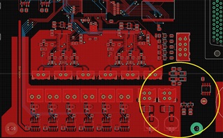
Here is my current status:

There are 6 high-side switches on the bottom of the picture (the SOIC-8 parts), each switching 24V / 0.4A. The high-side switches partially pulse the voltage and are controlled with a PWM (f < 1kHz). The high-side switches (connectors) unfortunately have to be placed this way due to mechanical conditions. The 24V supply comes from the top left und goes on the left down to the high-side switches (actually drawn in the top layer, not in the power layer). There are two ADS1248s above the high-side switches, each handling 3 PT100 sensors. The microcontroller is located above the ADS1248.
My current approach was to separate the ground (top layer) between the high-side switches and the analog front end of the ADS1248 in the layout. Does this make sense or would it be better to use a complete ground plane - both in the top and in the ground layer?