This thread has been locked.

If you have a related question, please click the "Ask a related question" button in the top right corner. The newly created question will be automatically linked to this question.

ADS131A04EVM: WREGS problem

Part Number: ADS131A04EVM

All:

I am debugging WREGS, and I am not seeing the registers written.

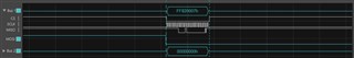
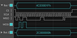
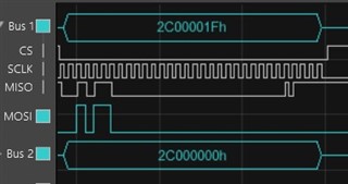
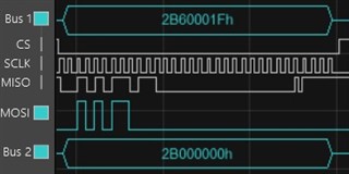
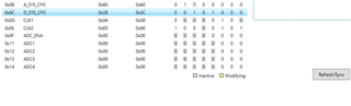
I have external 32-bit SPI running at 20 MHz, and I am sending the following, with CS active for entire 4 words:

0x6C030000  (WREGS, starting at location 0xC, write 4 registers)

0x3C020000 (D_SYS_CFG = 3C, CLK1 = 02)

0x480F0000 (CLK2 = 48, EN_ADC = 0F)

0x00000000 (CRC not used)

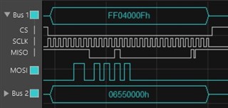
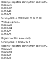
However, when I do a single RREG of 0xC to read the contents, I get value of 0. 

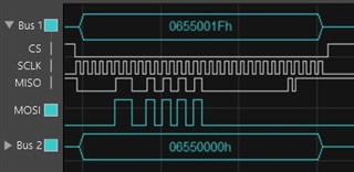
If I use single WREG command, I can write the proper values and read them back from the above registers.

I must be overlooking something - what am I doing wrong?

  • Hi Todd,

    what is the response word that you receive in the next frame? You should receive 0x4C030000.

    Note: if you are using the dynamic frame size and CRC is disabled (D_SYS_CFG[1:0] = 00b), you do not need to send the 0x00000000 CRC word.

    Regards,

    Ryan

  • Yes, I do receive 0x4C03000

    During that frame I send a RREG  0x2C000000, and the next frame shows 0x2C000000, where I would normally see 0x2C3C.

  • Hi Todd - I'm looking into this. Please note that the second byte in the response to the RREG command should always be 0x00. Therefore, you should be reading 0x3C00. 0x3C is also the default value for this register. Could you try sending RREG for 0Ch before writing?

    Regards,

    Ryan

  • I am including some screenshots:

    First is NULL being sent:

    Second is unlock. (Command on Bus2, Reply on Bus 1)

    Third is unlock received:

    Then, WWREGS to D_SYS_CFG, CLK1, CLK2, EN_ADC

    Then a read of D_SYS_CFG (response of previous was 4C03... as expected)

    And then a response of RREG:

    Just to show you single WREG works, here is A_SYS_CFG:

    And the response:

    Sorry for all of the screenshots, but so far, everything works well except for the WREGS command.

  • Hi Todd - it looks like something is pulling MISO high before the end of the frames (seems to be the last 4-5 bits). Most of the frames end with 0x0F or 0x1F at the end on Bus 1.

    The response in the third frame indicates the device was unlocked by the UNLOCK command sent in the second frame. The READY word was also output in the second frame (0xFF04), which is correct. This looks good so far (ignoring the end of Bus 1 for now).

    Then a read of D_SYS_CFG (response of previous was 4C03... as expected)

    And then a response of RREG:

    The response to WREGS looks correct (0x4C03). Instead of confirming by reading address 0Ch, can you read back 0Eh or 0Fh? Again, please read back a register which is written to a non-default value.

    Just to show you single WREG works, here is A_SYS_CFG:

    And the response:

    The fact that the WREG command (4Bxxh) was responded by (0x2Bxx) indicates that the command was received correctly. However, 0x60 is the default value for this register. Can you try sending 0x4B680000 to validate it is working?

    One other thought - please double-check your timing delays according to Figure 1. Especially the /CS falling edge to SCLK rising edge (td(CSSC) > 16 ns). 

    Regards,

    Ryan

  • Ryan:

    I changed the CS timing from 8 nsec to 18 nsec. I am still seeing the problem with WREGS. I do write and read back the ADC_EN (0x0F), so that WREG/RREG appears to be working. 

  • Hi Todd,

    Any luck with this yet? I've looped our digital designers into the thread to see what else we might be missing.

    Regards,

    Ryan

  • Ryan:

    I have not seen anything on my side that would account for the problem I am seeing with WREGS. BTW, I have not tried RREGS outside of getting ADC data from the device. Does WREGS work for you? (I should look at the interaction with the TIVO processor on the EVM, but from what I saw, setup was a single register at a time.) Thanks for tying in others.

  • Hi Todd,

    I couldn't acquire a logic analyzer capture since the EVM constantly polls for the STATUS response. However, I did test the WREGS and RREGS commands through our EVM GUI. The Console log and updated register map are captured below:

    Is Hamming Code enabled on your board? This is enabled by tying pin 32 high (M2). I'm not sure what else would cause the last 4-5 bits to toggle when using the 32-bit, LSB-padded word size.

    Regards,

    Ryan