This thread has been locked.

If you have a related question, please click the "Ask a related question" button in the top right corner. The newly created question will be automatically linked to this question.

ADS8584S: Different operation issues

Part Number: ADS8584S

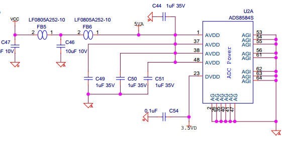
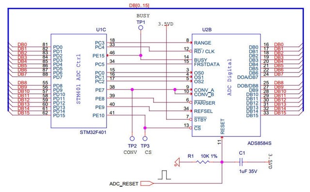
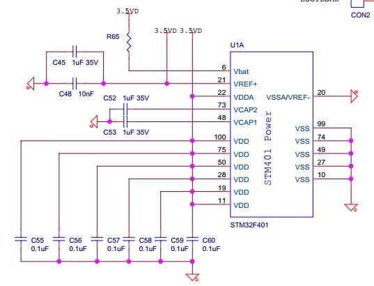
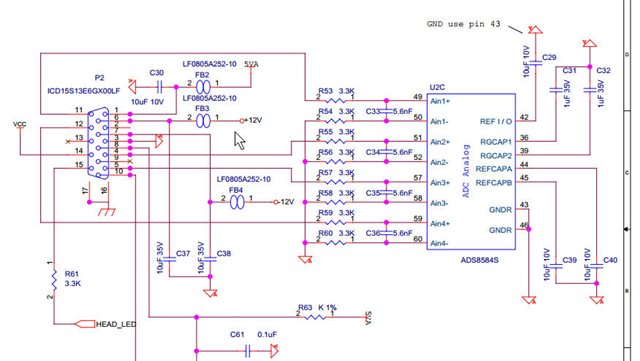
We use ADS8584S A/D converted in our project for analog measurements along with the STM32F401 MCU - the schematic design is attached

In our application the ADC is configured to work in parallel mode, +/-10V dynamic range, internal reference voltage of 10V, oversample between 0 and 4

Generally speaking the ADC works in the stable way with no missing code

We have several operation issues as explained hereunder:

1. BUSY signal - critical issue

--------------------------------------------------------------------------------

We use the threshold (MCU interrupt mode) to detect the start of conversion, after that to read the data from A/D

The high level of BUSY signal is approximately 1.7V, closed to MCU input threshold

To improve the threshold voltage we tried to add pull-up resistor between 20-3K, but the High level of the BUSY signal is not changed and is remained ~1.7V

Please, advise how to increase this signal voltage

2. Voltage calculation - critical

-----------------------------------------------------------------------

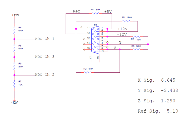
We have about 20% deviation offset between the calculated value and supplied known voltage

For example:

  • 597V supplied measured as 17,450 which means 5.325V
  • -2.597V supplied measured as -6,483 which means -1.978V

The deviation is slightly not linear

Please, explain how to calculate the analog data from the digital values to receive precise values


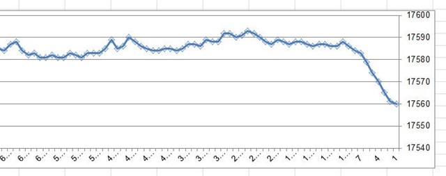
3. ADC in loop conversion - critical

------------------------------------------------------------------------

Running ADC conversion in loop with delay of 10 usec between each measurement, brings first 10-15 readings different from the rest of the of data. Delay of 10 sec and running again of the conversion in loop brings again about 10-15 not valid first readings. The data is presented on the graph attached

Please, explain how to fix it

  • Hi David,

    1. The digital high output on ADS8584S should be between 0.7xDVDD and DVDD+0.3, you are seeing lower level probably because the input on the MCU sinks higher current than 100uA. You can increase the DVDD voltage but it damage the IO of the MCU, the best way is using a single logic driver.

    2&3. Are you using a precision DC signal generator for the test? Can you provide the entire schematic including the circuit on the ADC’s input, REFIO and REFCAPA/B pins? Is there any connection between your GND_A and GND_D ground?

    Best regards,

    Dale

  • Dear Dale

    Thx a lot for your kind reply

    Attached please find the schematics of  the ADC inputs

    You can see there REFIO and REFCAPA/B 

    The connection between AGND and DGND via 0R resistor (2 different GND PCB layers).

    The analog signals to ADC from simple resistors dividers using +/-12V on the PCB (D-sub connector). Not very accurate signal but very stable.

    Will be happy to receive your feedback

    Thx in advance

    David

  • Hi David,

    I did not see a the resistor divider, what's the resistor value? The issue of invalid reading issue of first 10-15 should be caused by the large time constant which includes the 3.3kohm resistor/5.6nF cap in the filter and the large resistance and capacitance(10uF on +/-12V supplies) in the divider. Applying a DC precision signal to the RC filter directly can verify the issue, also reduce 3.3kohm and 5.6nF if needed.

    Best regards,

    Dale

  • Dear Dale

    Thx a lot for your kind reply

    1. You can see the dividers in the schematic drawing hereunder

    2. We will try to play with the values of RC filter

    3. Anyhow, we do not have a clear answer why the calculated values has a big offset and not linear behaviour

    Will be happy to get your opinion

    With best regards

    David


  • Hi David,

    Your 3.3kohm resistor forms a resistor divider with 1Mohm input impedance of the ADC, so it generates a gain error. There is a difference between your input signal and the voltage divided on ADC input. I do not know where your 597V or -2.597V signal applied for test, however any additional series resistor will make the difference worse.

    The resistance of your resistor divider are big and they are combined with the large resistance and capacitance in your RC filter to form a large time constant as a filter. When your signal is applied and conversion is started, it requires longer time to settle the signal, this is the reason why you saw the charging behavior at the beginning in your graph and why you got incorrect data reading for first 10-15 data.

    Best regards,

    Dale

  • Hi, Dale

    Sorry for late reply

    We have deviations of about 20% in the measured voltage

    You are right that we can improve the accuracy by modifying the input filter, but it will change the numbers by very low values (3.3kOhm relatively 1M – how big the deviation can be?)

    We made a try with 22Ohm resistor – no change in the results

    It looks that we are experiencing different type of problem

    Looking forward to hear about other ideas

    David

  • Hi David,

    Thanks for your response. I proposed to postpone the meeting to 10am today but did not get response. Please check with Yaron if you still want to discuss directly.

    I summarized the issues your have:

    a.  High level of BUSY is only 1.7V which is close to ST MCU input threshold:   The BUSY is an output signal from the ADC. As I said in my first response above, your MCU sinks more current than the specification, so a single logic driver was suggested. Also, I verified the BUSY signal on our EVM, it's higher than 2.3V while interfacing with FPGA.

    b.  Conversion code lower than analog input(e.g. -1.978V vs. -2.597V):   I need your clarification, did you compare the input voltage with the stable code or the first readings? your raw data will be very helpful. As I suggested above, it's good to use a DC precision generator instead of resistor divider for the test.

    c.  First 10-15 readings are incorrect:   This issue could be caused by the input or reference. I double checked your schematic. ADS8584S datasheet suggests to short REFCAPA and REFCAPB pins together and then decoupled to AGND using a 10uF capacitor, however a 10-uF capacitor for each pin was designed in your schematic, so the total capacitance on the reference buffer output is 20uF. The higher capacitance, the longer time to settle the reference voltage, this will influence the conversion code at the beginning. I suggest to  follow the datasheet by using only one 10uF then check the conversion code again.

        Regarding the error which is caused by higher series resistor on the ADC input, please see following application note:

        Reducing effects of external RC filter circuit on gain and drift error

    I'm looking forward to your feedback.

    Thanks&regards,

    Dale

  • Hi, Dale

    Thx a lot for your kind reply

    I would like to post hereunder the reply of our electronic engineer with more than 35 years experience in analog / digital electronics

    ================================

    1. You can find the data measured and calculated in the Excel file attached

    2. Regarding the data deviations of ~20%.

    The data can not deviate with ~20% because of 10uF on each reference voltage.

    Tests of ADC are performed when the ADC is configured by software as following: 10V range, parallel data, oversample 0-3, after that a loop of 100-200 samples. The readings were stable (few A/D points depend of oversample).

    The analog DC signals are constant from the resistor divider are non-accurate but stable (better than 1%).

    In my opinion, Using a resistor network can't cause a change in A/D reading of about 20%??  

    I do a lot of samples with different PCBs. The A/D results were very stable with identical measured values on different boards.

    Tests with 5V dynamic range were performed, and regarding data deviation the results were same.

    For example 10V range:

          Channel 1 – Input DC signal of 6.645V    17588 A/D points  Calculated  ~5.36V

          Channel 2 – Input DC signal of -2.438V   -6256 A/D points  Calculated  ~-1.90V

          Channel 3 – Input DC signal of 1.290V     3614  A/D points  Calculated  ~1.10V

    3. Regarding Busy signal. The input current of MCU  ports require less than 100uA. Other signals are OK.

    4. Regarding first 10-15 A/D readings, I have a question: The internal reference voltage is stable after ADC configuration or after start of conversion signal?

    =================================================

    Summarizing all the above, I think that in order to make faster decisions, we will be more than happy to have the conference call with you tomorrow

    With best regards

    DavidB1Os0D10UT1.xls

  • Dear Dale

    The main 2 issues of 20% deviation in AD calculated values & slow slop of first measurement was resolved by shortage between REFA and REFB pins.

    Thx a lot for your kind support, if we will need your further assistance we know how to find you :-)

    We can cancel our today conference call - we do not have anything else to say

    Thx again and regards

    David