Other Parts Discussed in Thread: LMK61E2, LMX2594, , , ADC12DJ3200
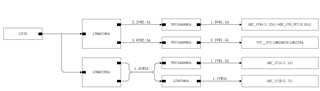
- ADC2DJ5200RF diagram:
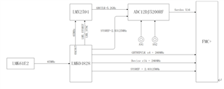
2.Configuration mode:
LMK61E2:Fout = 65MHz;
LMK04828B:DCLK=260MHz; SCLK=2.03125MHz, continuous mode;
LMX2594:RoutA = 5200MHz, RoutB not used;
ADC12DJ5200RF:JMODE=1, Fs=10400MSPS;
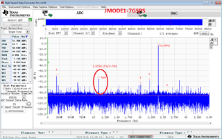
3.Questions:
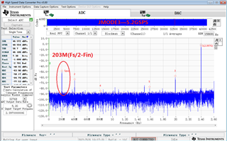
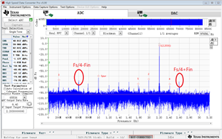
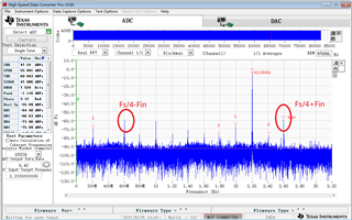
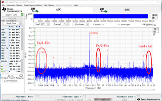
- As shown in the figure below, Fs/4±Fin and Fs/2-Fin have large interweaving spurs, which leads to unsatisfactory indicators; what may be the cause, is there any way to improve。
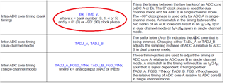
- When other registers can be read and written normally, we try to adjust the value of register Bx_TIME_y, but the read value is still the default value and cannot be modified; can we modify the register value of Bx_TIME_y?