


Hello!
Tell me, please, what could be the problem.
I have a issue getting data if the PGA is activated.
Register configuration by default, I only change the gain.
To registers 0-3, values are written and read correctly.
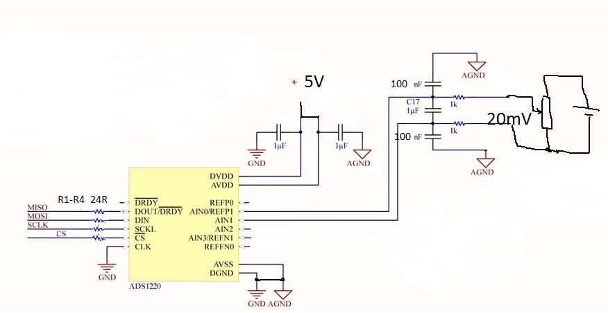
I connect the voltage from the battery to the input through a divider, about
20.6 mV, but I get this value only if the PGA bypass is on.
Values 20.65335, 20.65421, 20.65333, 20.65112, etc.
If the PGA bypass is turned off and set PGA to anything gain, I get very small floating values (0.00012, 0.00015, -0.00010, -0.00013, etc)
Maybe I'm doing something wrong?
Below I attached schematic, logic analizer screenshot, arduino code and lib
what I use.
Code
#include "ADS1220.h"
ADS1220 adc;
#define PGA          1
#define VREF         2.048
#define VFSR         VREF/PGA
#define FULL_SCALE   (((long int)1<<23)-1)


void setup() {
  Serial.begin(9600);
  adc.begin(9, 8);
  adc.setGain(PGA);
  adc.setConversionMode(1); //continious mode
  adc.setMultiplexer(0X00);
  adc.setPGAbypass(true); //PGA OFF

  uint8_t Buff = 0;
  Buff = adc.readRegister(0);
  Serial.print("REG0 = ");
  Serial.println(Buff, BIN);
  Buff = adc.readRegister(1);
  Serial.print("REG1 = ");
  Serial.println(Buff, BIN);
  Buff = adc.readRegister(2);
  Serial.print("REG2 = ");
  Serial.println(Buff, BIN);
  Buff = adc.readRegister(3);
  Serial.print("REG3 = ");
  Serial.println(Buff, BIN);
}

void loop() {
  char outstr[10];

  if (adc.isDataReady()) {
    long test = adc.readADC();
    float a = convertToMilliV(test);
    dtostrf(a, 10, 5, outstr);
    Serial.println(outstr);
  }
  delay(300);
}

float convertToMilliV(int32_t i32data)
{
  return (float)((i32data * VFSR * 1000) / FULL_SCALE);
}

CPP file

#include "ADS1220.h"
#include "Arduino.h"
#include "SPI.h"

ADS1220::ADS1220() {
}

void ADS1220::writeRegister(uint8_t address, uint8_t value) {
  digitalWrite(ADS1220_CS_PIN, LOW);
  SPI.transfer(CMD_WREG|(address<<2)); // What not setting num bytes?
  SPI.transfer(value);
  startSync(); // Send start/sync for continuous conversion mode
  delayMicroseconds(1); // Delay a minimum of td(SCCS)
  digitalWrite(ADS1220_CS_PIN, HIGH);
}

uint8_t ADS1220::readRegister(uint8_t address) {
  digitalWrite(ADS1220_CS_PIN,LOW);
  SPI.transfer(CMD_RREG|(address<<2)); // What not setting num bytes?
  uint8_t data = SPI.transfer(SPI_MASTER_DUMMY);
  digitalWrite(ADS1220_CS_PIN,HIGH);
  return data;
}

void ADS1220::begin(uint8_t cs_pin, uint8_t drdy_pin) {
  // Set pins up
  ADS1220_CS_PIN = cs_pin;
  ADS1220_DRDY_PIN = drdy_pin;

  // Configure the SPI interface (CPOL=0, CPHA=1)
  SPI.begin();
  SPI.setBitOrder(MSBFIRST);
  SPI.setDataMode(SPI_MODE1);

  // Configure chip select as an output
  pinMode(ADS1220_CS_PIN, OUTPUT);

  // Configure DRDY as as input (mfg wants us to use interrupts)
  pinMode(ADS1220_DRDY_PIN, INPUT);

  digitalWrite(ADS1220_CS_PIN, LOW); // Set CS Low
  delayMicroseconds(100); // Wait a minimum of td(CSSC)
  reset(); // Send reset command
  delayMicroseconds(100);; // Delay a minimum of 50 us + 32 * tclk

  // Sanity check read back (optional)

  startSync(); // Send start/sync for continuous conversion mode
  delayMicroseconds(1); // Delay a minimum of td(SCCS)
  digitalWrite(ADS1220_CS_PIN, HIGH); // Clear CS to high
}

bool ADS1220::isDataReady() {
  if (digitalRead(ADS1220_DRDY_PIN) == HIGH) {
    return false;
  }
  return true;
}

long ADS1220::readADC() {
  digitalWrite(ADS1220_CS_PIN, LOW); // Take CS low
  delayMicroseconds(1); // Minimum of td(CSSC)
  long adcVal = SPI.transfer(SPI_MASTER_DUMMY);
  adcVal = (adcVal << 8) | SPI.transfer(SPI_MASTER_DUMMY);
  adcVal = (adcVal << 8) | SPI.transfer(SPI_MASTER_DUMMY);
  adcVal = ( adcVal << 8 );
  adcVal = ( adcVal >> 8 );
  delayMicroseconds(1); // Minimum of td(CSSC)
  digitalWrite(ADS1220_CS_PIN, HIGH);
  return adcVal;
}

byte * ADS1220::readADC_Array() {
  digitalWrite(ADS1220_CS_PIN, LOW); // Take CS low
  delayMicroseconds(1); // Minimum of td(CSSC)
  static byte dataarray[3];
  for (int x = 0; x < 3 ; x++)
  {
    dataarray[x] = SPI.transfer(SPI_MASTER_DUMMY);
  }
  delayMicroseconds(1); // Minimum of td(CSSC)
  digitalWrite(ADS1220_CS_PIN, HIGH);
  return dataarray;
}

//Single Conversion read modes
long ADS1220::readADC_Single() {
  digitalWrite(ADS1220_CS_PIN, LOW); // Take CS low
  delayMicroseconds(1); // Minimum of td(CSSC)

  SPI.transfer(0x08);
  while(digitalRead(ADS1220_DRDY_PIN) == HIGH)
  {
    //Wait to DRDY goes down
    //Not a good thing
    //Code could be stuck here
    //Need a improve later
  }

  long adcVal = SPI.transfer(SPI_MASTER_DUMMY);
  adcVal = (adcVal << 8) | SPI.transfer(SPI_MASTER_DUMMY);
  adcVal = (adcVal << 8) | SPI.transfer(SPI_MASTER_DUMMY);

  adcVal = ( adcVal << 8 );
  adcVal = ( adcVal >> 8 );
  delayMicroseconds(1); // Minimum of td(CSSC)
  digitalWrite(ADS1220_CS_PIN, HIGH);
  return adcVal;
}

byte * ADS1220::readADC_SingleArray() {
  digitalWrite(ADS1220_CS_PIN, LOW); // Take CS low
  delayMicroseconds(1); // Minimum of td(CSSC)

  SPI.transfer(0x08);
  while(digitalRead(ADS1220_DRDY_PIN) == HIGH)
  {
    //Wait to DRDY goes down
    //Not a good thing
    //Code could be stuck here
    //Need a improve later
  }

  static byte dataarray[3];
  for (int x = 0; x < 3 ; x++)
  {
    dataarray[x] = SPI.transfer(SPI_MASTER_DUMMY);
  }
  delayMicroseconds(1); // Minimum of td(CSSC)
  digitalWrite(ADS1220_CS_PIN, HIGH);
  return dataarray;
}

void ADS1220::sendCommand(uint8_t command) {
  // Following Protocentral's code, not sure exactly what's going on here.
  digitalWrite(ADS1220_CS_PIN, LOW);
  delay(2);
  digitalWrite(ADS1220_CS_PIN, HIGH);
  delay(2);
  digitalWrite(ADS1220_CS_PIN, LOW);
  delay(2);
  SPI.transfer(command);
  delay(2);
  digitalWrite(ADS1220_CS_PIN, HIGH);
}

void ADS1220::writeRegisterMasked(uint8_t value, uint8_t mask, uint8_t address) {
  // Write the value to a register using the mask to leave the rest of the
  // register untouched. This does not shift the value, so it shoudl be provided
  // shifted to the appropriate positions.

  // Read what's in the register now
  uint8_t register_contents = readRegister(address);

  // Flip the mask so that it's zeros where we'll put data and zero out that
  // part of the register's contents
  register_contents = register_contents & ~mask;

  // OR in the value to be written
  register_contents = register_contents | value;

  // Write it back out
  writeRegister(address, register_contents);
}

void ADS1220::setMultiplexer(uint8_t value) {
  /* Set multiplexer

  | Value | AINp | AINn |
  | ----- | ---- | ---- |
  | 0x00  | AIN0 | AIN1 |
  | 0X01  | AIN0 | AIN2 |
  | 0X02  | AIN0 | AIN3 |
  | 0X03  | AIN1 | AIN2 |
  | 0X04  | AIN1 | AIN3 |
  | 0X05  | AIN2 | AIN3 |
  | 0X06  | AIN1 | AIN0 |
  | 0X07  | AIN3 | AIN2 |
  | 0X08  | AIN0 | AVSS |
  | 0X09  | AIN1 | AVSS |
  | 0X0A  | AIN2 | AVSS |
  | 0X0B  | AIN3 | AVSS |
  | 0X0C  |  REF/4 MON  |
  | 0X0D  | APWR/4 MON  |
  | 0X0E  |   SHORTED   |
  */
  // Make sure the value is in the valid range. Otherwise set to 0x00
  if (value > 0x0E) {
    value = 0x00;
  }
  value = value << 4; // Shift to match with mask
  writeRegisterMasked(value, REG_MASK_MUX, CONFIG_REG0_ADDRESS);
}

void ADS1220::setGain(uint8_t gain) {
  /* Sets ADC gain. Possible values are 1, 2, 4, 8, 16, 32, 64, 128. */
  uint8_t value = 0x00;
  switch(gain) {
    case 1:
      value = 0x00;
      break;
    case 2:
      value = 0x01;
      break;
    case 4:
      value = 0x02;
      break;
    case 8:
      value = 0x03;
      break;
    case 16:
      value = 0x04;
      break;
    case 32:
      value = 0x05;
      break;
    case 64:
      value = 0x06;
      break;
    case 128:
      value = 0x07;
      break;
    default:
      value = 0x00;
      break;
  }
  value = value << 1; // Shift to match with mask
  writeRegisterMasked(value, REG_MASK_GAIN, CONFIG_REG0_ADDRESS);
}

void ADS1220::setPGAbypass(bool value) {
  /* Bypasses the PGA if true.
     PGA can only be disabled for gains 1, 2, 4.
  */
  writeRegisterMasked(value, REG_MASK_PGA_BYPASS, CONFIG_REG0_ADDRESS);
}

void ADS1220::setDataRate(uint8_t value) {
  /* Sets the data rate for the ADC. See table 18 in datasheet for datarates
     in various operating modes. */
  // Make sure the value is in the valid range. Otherwise set to 0x00
  if (value > 0x07) {
    value = 0x00;
  }
  value = value << 5; // Shift to match with mask
  writeRegisterMasked(value, REG_MASK_DATARATE, CONFIG_REG1_ADDRESS);
}

void ADS1220::setOpMode(uint8_t value) {
  /* Sets the ADC operating mode:
     0 - Normal mode
     1 - Duty-cycle mode
     2 - Turbo mode
  */
  // Make sure the value is in the valid range. Otherwise set to 0x00
  if (value > 0x02) {
    value = 0x00;
  }
  value = value << 3; // Shift to match with mask
  writeRegisterMasked(value, REG_MASK_OP_MODE, CONFIG_REG1_ADDRESS);
}

void ADS1220::setConversionMode(uint8_t value) {
  /* Sets the ADC conversion mode.
     0 - Single shot mode
     1 - continuous conversion mode
  */
  // Make sure the value is in the valid range. Otherwise set to 0x00
  if (value > 0x01) {
    value = 0x00;
  }
  value = value << 2; // Shift to match with mask
  writeRegisterMasked(value, REG_MASK_CONV_MODE, CONFIG_REG1_ADDRESS);
}

void ADS1220::setTemperatureMode(uint8_t value) {
  /* Controls the state of the internal temperature sensor.
     0 - Disables temperature sensor
     1 - Enables temperature sensor
  */
  // Make sure the value is in the valid range. Otherwise set to 0x00
  if (value > 0x01) {
    value = 0x00;
  }
  value = value << 1; // Shift to match with mask
  writeRegisterMasked(value, REG_MASK_TEMP_MODE, CONFIG_REG1_ADDRESS);
}

void ADS1220::setBurnoutCurrentSources(bool value) {
  /* Turns the 10uA burn-out current sources on or off. */
  writeRegisterMasked(value, REG_MASK_BURNOUT_SOURCES, CONFIG_REG1_ADDRESS);
}

void ADS1220::setVoltageRef(uint8_t value) {
  /* Sets the voltage reference used by the ADC.
     0 - Internal 2.048 V
     1 - External on REFP0 and REFN0 inputs
     2 - External on AIN0/REFP1 and AIN3/REFN1 inputs
     3 - Use analog supply as reference
  */
  // Make sure the value is in the valid range. Otherwise set to 0x00
  if (value > 0x03) {
    value = 0x00;
  }
  value = value << 6; // Shift to match with mask
  writeRegisterMasked(value, REG_MASK_VOLTAGE_REF, CONFIG_REG2_ADDRESS);
}

void ADS1220::setFIR(uint8_t value) {
  /* Controls the FIR filter on the ADC.
     0 - No 50 or 60 Hz rejection
     1 - Both 50 and 60 Hz rejection
     2 - 50 Hz rejection
     3 - 60 Hz rejection
  */
  // Make sure the value is in the valid range. Otherwise set to 0x00
  if (value > 0x03) {
    value = 0x00;
  }
  value = value << 4; // Shift to match with mask
  writeRegisterMasked(value, REG_MASK_FIR_CONF, CONFIG_REG2_ADDRESS);
}

void ADS1220::setPowerSwitch(uint8_t value) {
  /* Configures behavior of low-side switch between AIN3/REFN1 and AVSS.
     0 - Always open
     1 - Automatically closes when START/SYNC command is sent and opens when
         POWERDOWN command is issues.
  */
  // Make sure the value is in the valid range. Otherwise set to 0x00
  if (value > 0x01) {
    value = 0x00;
  }
  value = value << 3; // Shift to match with mask
  writeRegisterMasked(value, REG_MASK_PWR_SWITCH, CONFIG_REG2_ADDRESS);
}

void ADS1220::setIDACcurrent(uint8_t value) {
  /* Set current for both IDAC1 and IDAC2 excitation sources.
     0 - Off
     1 - 10 uA
     2 - 50 uA
     3 - 100 uA
     4 - 250 uA
     5 - 500 uA
     6 - 1000 uA
     7 - 1500 uA
  */
  // Make sure the value is in the valid range. Otherwise set to 0x00
  if (value > 0x07) {
    value = 0x00;
  }
  writeRegisterMasked(value, REG_MASK_IDAC_CURRENT, CONFIG_REG2_ADDRESS);
}

void ADS1220::setIDAC1routing(uint8_t value) {
  /* Selects where IDAC1 is routed to.
     0 - Disabled
     1 - AIN0/REFP1
     2 - AIN1
     3 - AIN2
     4 - AIN3/REFN1
     5 - REFP0
     6 - REFN0
  */
  // Make sure the value is in the valid range. Otherwise set to 0x00
  if (value > 0x06) {
    value = 0x00;
  }
  value = value << 5; // Shift to match with mask
  writeRegisterMasked(value, REG_MASK_IDAC1_ROUTING, CONFIG_REG3_ADDRESS);
}

void ADS1220::setIDAC2routing(uint8_t value) {
  /* Selects where IDAC2 is routed to.
     0 - Disabled
     1 - AIN0/REFP1
     2 - AIN1
     3 - AIN2
     4 - AIN3/REFN1
     5 - REFP0
     6 - REFN0
  */
  // Make sure the value is in the valid range. Otherwise set to 0x00
  if (value > 0x06) {
    value = 0x00;
  }
  value = value << 2; // Shift to match with mask
  writeRegisterMasked(value, REG_MASK_IDAC2_ROUTING, CONFIG_REG3_ADDRESS);
}

void ADS1220::setDRDYmode(uint8_t value) {
  /* Controls the behavior of the DOUT/DRDY pin when new data are ready.
     0 - Only the dedicated DRDY pin is used
     1 - Data ready indicated on DOUT/DRDY and DRDY
 */
  // Make sure the value is in the valid range. Otherwise set to 0x00
  if (value > 0x01) {
    value = 0x00;
  }
  value = value << 1; // Shift to match with mask
  writeRegisterMasked(value, REG_MASK_DRDY_MODE, CONFIG_REG3_ADDRESS);
}

void ADS1220::reset() {
  sendCommand(CMD_RESET);
}

void ADS1220::startSync() {
  sendCommand(CMD_START_SYNC);
}

void ADS1220::powerDown() {
  sendCommand(CMD_PWRDWN);
}

void ADS1220::rdata() {
  sendCommand(CMD_RDATA);
}

void ADS1220::ReadRegister(int StartAddress, int NumRegs, unsigned * pData)
{
   int i;

		digitalWrite(ADS1220_CS_PIN, LOW);

    // send the command byte
    SendByte(CMD_RREG | (((StartAddress<<2) & 0x0c) |((NumRegs-1)&0x03)));

    // get the register content
    for (i=0; i< NumRegs; i++)
    {
        *pData++ = ReceiveByte();
    }
		digitalWrite(ADS1220_CS_PIN, HIGH);

    return;
}

void ADS1220::SendByte(unsigned char Value)
{
    SPI.transfer(Value);
}

unsigned int ADS1220::ReceiveByte(void)
{
  unsigned int readvalue;
  readvalue =  SPI.transfer(0x00);
  return readvalue;
}
header file
#ifndef ADS1220_h
#define ADS1220_h

#include "Arduino.h"

#define SPI_MASTER_DUMMY   0xFF
// Commands for the ADC
#define CMD_RESET 0x07
#define CMD_START_SYNC 0x08
#define CMD_PWRDWN 0x03
#define CMD_RDATA 0x1f
#define CMD_RREG 0x20
#define CMD_WREG 0x40

// Configuration registers
#define CONFIG_REG0_ADDRESS 0x00
#define CONFIG_REG1_ADDRESS 0x01
#define CONFIG_REG2_ADDRESS 0x02
#define CONFIG_REG3_ADDRESS 0x03

// Register masks for setings
// Register 0
#define REG_MASK_MUX 0xF0
#define REG_MASK_GAIN 0x0E
#define REG_MASK_PGA_BYPASS 0x01

// Register 1
#define REG_MASK_DATARATE 0xE0
#define REG_MASK_OP_MODE 0x18
#define REG_MASK_CONV_MODE 0x04
#define REG_MASK_TEMP_MODE 0x02
#define REG_MASK_BURNOUT_SOURCES 0x01

// Register 2
#define REG_MASK_VOLTAGE_REF 0xC0
#define REG_MASK_FIR_CONF 0x30
#define REG_MASK_PWR_SWITCH 0x08
#define REG_MASK_IDAC_CURRENT 0x07

// Register 3
#define REG_MASK_IDAC1_ROUTING 0xE0
#define REG_MASK_IDAC2_ROUTING 0x1C
#define REG_MASK_DRDY_MODE 0x02
#define REG_MASK_RESERVED 0x01

class ADS1220 {
  public:
    ADS1220();
    uint8_t ADS1220_CS_PIN;
    uint8_t ADS1220_DRDY_PIN;
    void writeRegister(uint8_t address, uint8_t value);
    uint8_t readRegister(uint8_t address);
    void begin(uint8_t cs_pin, uint8_t drdy_pin);
    bool isDataReady(void);
    long readADC(void);
    byte * readADC_Array(void);
    long readADC_Single(void);
    byte * readADC_SingleArray(void);
    void sendCommand(uint8_t command);
    void reset(void);
    void startSync(void);
    void powerDown(void);
    void rdata(void);
    void writeRegisterMasked(uint8_t value, uint8_t mask, uint8_t address);
    void setMultiplexer(uint8_t value);
    void setGain(uint8_t gain);
    void setPGAbypass(bool value);
    void setDataRate(uint8_t value);
    void setOpMode(uint8_t value);
    void setConversionMode(uint8_t value);
    void setTemperatureMode(uint8_t value);
    void setBurnoutCurrentSources(bool value);
    void setVoltageRef(uint8_t value);
    void setFIR(uint8_t value);
    void setPowerSwitch(uint8_t value);
    void setIDACcurrent(uint8_t value);
    void setIDAC1routing(uint8_t value);
    void setIDAC2routing(uint8_t value);
    void setDRDYmode(uint8_t value);

	void SendByte(unsigned char cData );     // Send byte to the ADS1220
    unsigned int ReceiveByte(void);          // Receive byte from the ADS1220
	int GetChannel(void);
	void ReadRegister(int StartAddress, int NumRegs, unsigned * pData);
  };
#endif


