This thread has been locked.

If you have a related question, please click the "Ask a related question" button in the top right corner. The newly created question will be automatically linked to this question.

ADS54J60: DC-coupling, large dc level component in the input signal resulting in a ripple in the sampling output

Part Number: ADS54J60
Other Parts Discussed in Thread: LMH6552

Hello, I saw your question in the forum, and now I have the same problem as you.

https://e2e.ti.com/support/data-converters/f/73/t/660047

My main references: tidub15, tidubh9.

Hello, I am debugging the board of ADS54J60. PCB is drawn by myself. Using DC coupling mode and LMH6552 operational amplifier, which converted the single-ended signal into differential signal, which is supplied to ADS54J60 for sampling.

When the input signal is collected by ADC, problems are encountered at present. The problem is described as follows. When the input signal has no DC level component or the DC level component is very small, the sampling of ADS54J60 is normal. Once the DC level component in the signal is large, or the bias voltage is large, the ripple will occur. The ripple frequecy is 1/4 of the sampling clock frequency of ADC, and the ripple amplitude is 0-512, [8:0]. (Tests at 1GHz and 750MHz, respectively, yielded similar results)

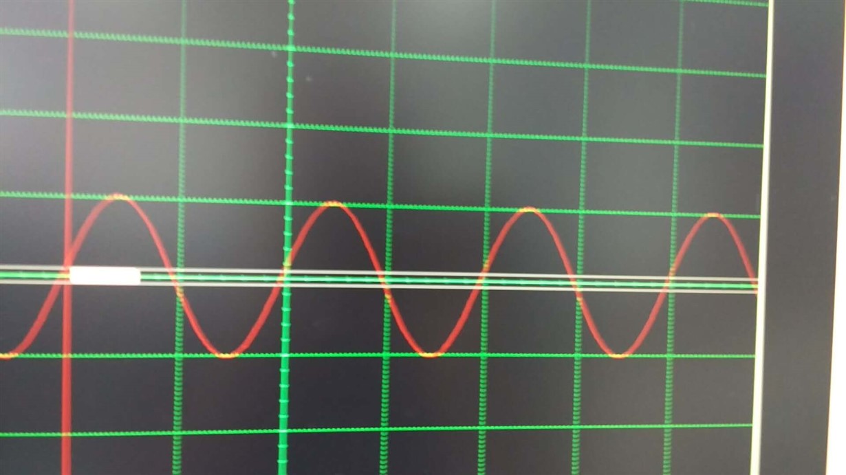
here followed the normal sampling waveform

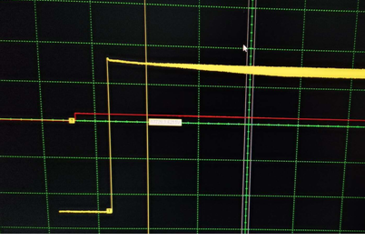
This is a process of ripple shock when the signal has a relatively large DC level component. Please note that the DC level component causes the onset of the earthquake. The time of shock stabilization is about 35us. as followed the ripple shock waveform

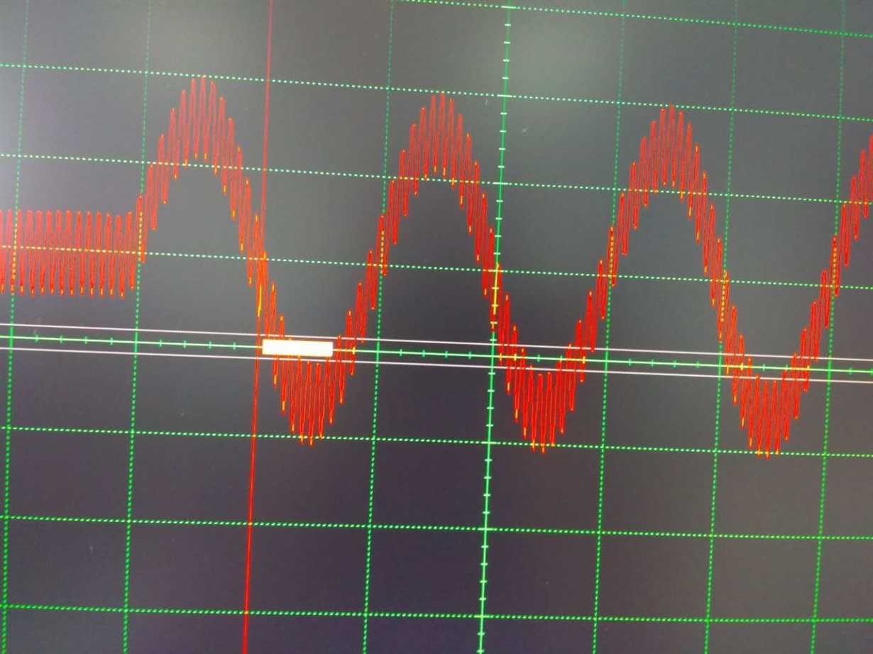
the detailed ripple waveform is followed 

I found that the current ripple waveform amplitude has nothing to do with the waveform shape and waveform amplitude. The ripple frequency is 1/4 of the sampling clock frequency of ADC. It feels that it is not a problem on the analog signal conditioning link.

I got confused, help please~

  • User,

    Please see section 9.1.4 of the latest version of the ADC54J60 data sheet (SBAS706D April 2019). You may need to freeze the DC offset correction function of the device.

    Regards,

    Jim

  • thanks for your advice Jim,

    I've tried, and I've tested a variety of models. Including the version of SBAS706B,

    this test will not work without paying attention to "DC offset correction function".

    here is the result:

    Enabling "freeze DC offset correction function" and not enabling "Bypass Correction", this field test is not feasible. Enabling both "freeze DC offset correction function" and "Bypass Correction", this field test is not feasible,either.

    However, There is another problem.:

    there's a register, 6A00, 012h register bit-1, which is described on the datasheet as always write 1().

    It seems that this is not the case through testing.

    the result comes from my test is that  the initialization sequence given in the manual did not write that the register had to be configured. In fact, not configuring 1 would work properly, but configuring 1 would not work properly.

    I don't whether I make myself clear or not, 

    I hope u can help me, Thanks a lot!

  • Hi~ Jim  me again~

    There're some questions about the DC offset:

    Does ADC's DC offset work by default? is it always being corrected?

    According to the manual, it should not work all the time. Otherwise, there is no need to manually correct the drift caused by temperature?

    Furthermore, the manual tells us that DC Offset correction of ADC is only for AC coupling, and freeze function should be enabled for DC coupling. According to the actual test, the ADC can not work properly while enabling freeze function and disable bypass fuction. There are 6100h, 68h, bit-1, always write 1, I have tried, if bit-1, always write 1, ADC can not work properly, it is not clear what caused this?

    I bought the chips in August last year, Does the newest Configuration file still work on it?

    the recommended Work Mode 8224 configuration given in the datasheet is so hard to understand,

    any simplify register configuration?

    looking for your reply~

  • User,

    The configuration file used by the GUI for mode 8824 is attached.  Make sure to always issue a hard reset to the device after the clocks are present.

    The DC correction is enabled by default. The user should only have to correct for offset drift if they have this function disabled.

    The latest configuration files will work with the devices you purchased.

    What doesn't work when you set bit 1 high in address 0x68 of page 6100? I do not see this issue with our setup when using the 8224 configuration.

    Regards,

    Jim

    SPI writes for 8224 mode.docx

  • Hi Jim~ 

    I tried some other tests, There are still some problems in the debugging process. Could you please help me to solve them?

    Is a hard reset necessary for the ADC

    What's the difference between 'must wire 1/0' and 'always write 1/0' described in the datasheet?

    Is it OK that 'always write 1/0' acceptable by default? For example, 6800h-42h-bit [7:3] must write 0 (default value is 5'b0), 6A00h-12h-bit [1] always write 1 (default value is 1'b0).

    When is freeze offset correction (68h, bit-7) under DC coupling? When is bypass offset correction (68h, bit-1) under DC coupling?

    When external correction shall be used? Will it run on power or after ADC works stably? If external correction is not properly configured, will it affect the normal working state of ADC? In the start-up sequence (9.1.1), there is no mention of external correction at all. In Effect of Temperature (9.1.4.2), although the use of external correction is mentioned, there is no mention of when to correct it. How to configure the 61000000h-68h registers when using external correction?

    After I configure the DC offset corr of ADC, I found that the 204b link can be connected normally (observed by ILA), but the ADC is not working properly. When DC offset is not configured, ADC works normally, that is, there will be noise similar to ripple after DC offset. I feel related to the above questions. Please help me to solve them.

    looking for your reply

  • Hi~ Jim

    According to the description in the manual, the difference between DC coupling and AC coupling is only the setting of 001180h-4Fh-bit [0]? According to the description, it is only the difference of series resistance of vcm. What's more, the resistance termination and anti-aliasing filter design given in the manual and EVM are all based on the series resistance under AC coupling? So, can we configure ADC as AC coupling mode and work in DC coupling mode?

    Is there a mandatory order to configure registers? My configuration sequence, configuration clock in a stable working state, then configuration ADC work, after the completion of ADC configuration, configure clock to generate sysref pulse, establish 204b link connection. I also tried another configuration sequence. First, I configure the clock to work stably. Then I configure the ADC register partially. Then I configure the clock to generate sysref pulses and establish a 204b link connection. Then I configure the DC offset correction of the ADC.

    Personally, DC offset correction is more troublesome, once the configuration is not good, it directly affects the stable working state of ADC. How should DC offset correction be configured in DC coupling mode? After the sysref pulse, wait for the stable connection of 204b link, then DC offset correction? Or does ADC work in AC coupling mode, complete DC offset correction, and then change to DC coupling mode?

    What's more, you said that DC offset correction is always working, "The DC correction is enabled by default. The user should only have to correct for offset drift if they have this function disabled". Since DC offset correction is working all the time, it can also be calibrated in real time with the change of temperature. Why do you need to calibrate it manually (9.1.4.2)?

    Looking for your reply~

  • User,

    Is a hard reset necessary for the ADC?

    Yes. Do this after the clocks are present.

    What's the difference between 'must wire 1/0' and 'always write 1/0' described in the datasheet?

    No difference.

    Is it OK that 'always write 1/0' acceptable by default? For example, 6800h-42h-bit [7:3] must write 0 (default value is 5'b0), 6A00h-12h-bit [1] always write 1 (default value is 1'b0).

    Not sure what you are asking. If the part defaults with a "1" after reset, there is no need to do these writes.

    When is freeze offset correction (68h, bit-7) under DC coupling? When is bypass offset correction (68h, bit-1) under DC coupling?

    See section 9.1.4 of the data sheet. 

    When external correction shall be used? Will it run on power or after ADC works stably? If external correction is not properly configured, will it affect the normal working state of ADC? In the start-up sequence (9.1.1), there is no mention of external correction at all. In Effect of Temperature (9.1.4.2), although the use of external correction is mentioned, there is no mention of when to correct it. How to configure the 61000000h-68h registers when using external correction? See Table 77.

    After I configure the DC offset corr of ADC, I found that the 204b link can be connected normally (observed by ILA), but the ADC is not working properly. When DC offset is not configured, ADC works normally, that is, there will be noise similar to ripple after DC offset. I feel related to the above questions. Please help me to solve them.

    Send me the register writes you are doing to cause this.

    Regards,

    Jim

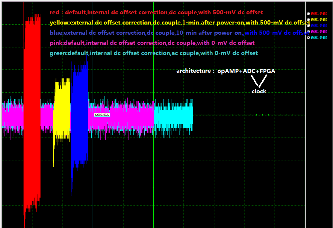
  • This is the result I got recently.

    The internal DC error calibration module works normally under AC or DC coupling and without DC bias.

    In the case of DC coupling with DC bias, the internal DC error calibration module of ADS54J60 can not work properly at this time, which will lead to large errors.According to your suggestion and the description in the latest manual, the internal DC error correction is carried out during the power-on configuration process, the internal DC error correction module is closed after the configuration is completed, and the external DC error correction is carried out by using the last internal DC error correction value. The image results show that the external correction will introduce more noise than the internal correction.

    This is the best way I can think of at present.

  • User,

    To me it appears the external calibration (blue) is much better than the internal (red). Not sure why you said it is the other way around.

    Please remove the input to the ADC, do a DC offset calibration, freeze the calibration, then turn on the input. Over time, repeat these steps to do a calibration to compensate for temperature drifts of the part.

    Regards,

    Jim