This thread has been locked.

If you have a related question, please click the "Ask a related question" button in the top right corner. The newly created question will be automatically linked to this question.

TINA/Spice/UCC27714: HS pin passing high voltage into HO output pin

Guru 54568 points
Part Number: UCC27714
Other Parts Discussed in Thread: TINA-TI

Tool/software: TINA-TI or Spice Models

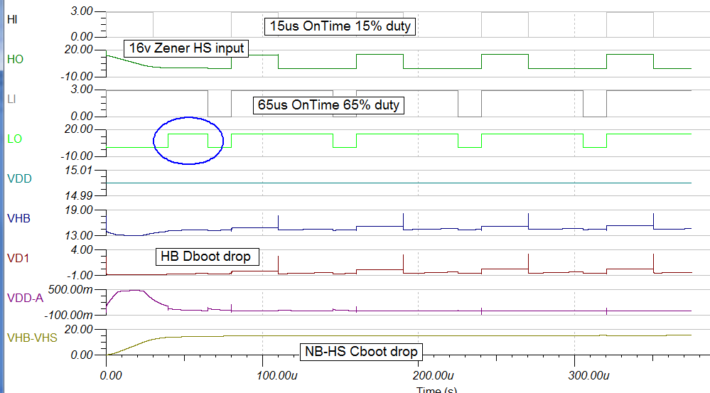
Issue of HS pin passing 1/2 bridge high voltage out the HO pin and compressing the HO signal in plot output when not arrested via added 16v zener on HS pin.

HS pin is connected to high side NFET source leading into drain at low side NFET, 1/2 bridge layout. Also have initial rouge pulse (blue oval) showing up in the LO output when 2 signal generators at different duty cycles are producing drive signals into HI/LI inputs, 80us period.  

Is the HS pin passing high voltage out HO pin (+160v not shown) expected to occur in production chips? 

Any idea what would cause the HO output to produce an initial rouge pulse as below capture shows?

Thanks,


  • Hi BP101,

    We will look into this, but before that, can you share your exact TSC file with us? You can find some more information here: e2e.ti.com/.../592360. This will help us debug this faster and more efficiently.

    Thanks!
  • Hi Nikhil,

    Sure the modified TSC is zipped below. The original TSC download HI/LI inputs had a single high frequency generator. Simulation of HO/LO would take a long time to start producing signals, far more than 90ns propagation delay & large void would occur between input to output signals.

    My simulation produces 80us periods with longer on time of the low side. If you remove the zener diode from HS pin you will see voltage on HO try to match the potential of HS. Was more interested in measuring the VDD current of Dboot,Cboot charge pump with HO/LO outputs driving NFET gate loads. Connecting the HO/LO gate drive output resistors to ground the VDD current through Dboot increases.  Seemingly we should be able to measure HO/LO gate drive current via resistors tied to ground. That is keeping HI/LI PWM pulse <10us and maintain 2.5 amps, 4amps MAX. I have not yet verified if the Tina model can do that.

    /cfs-file/__key/communityserver-discussions-components-files/234/Test-UCC27714.zip


  • Hi BP101,

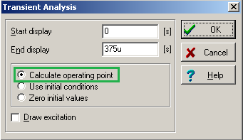
    Please select "Calculate operating point" in transient analysis window and hit OK to simulate the test bench as shown below 

    Below is the simulation result with the above simulation setting.

    Thanks & Regards,

    Arpan Gupta

  • Hi Arpan,

    Excellent the phantom pulse goes away but also notice ADD-Amps is now producing an odd range of start up milliamps.

    Any luck to stop the high voltage at HO output with initial conditions checked?

    It seems the HS input bias is not actually above VSS/COM or (floating) when we check initial conditions as the instructions suggest?

  • Hi BP101,

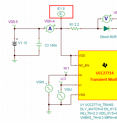
    Please remove the IC1 from input side(which is shown below). As VDD is DC and placing IC=0 causes large VDD-Amps to flow.
     
     
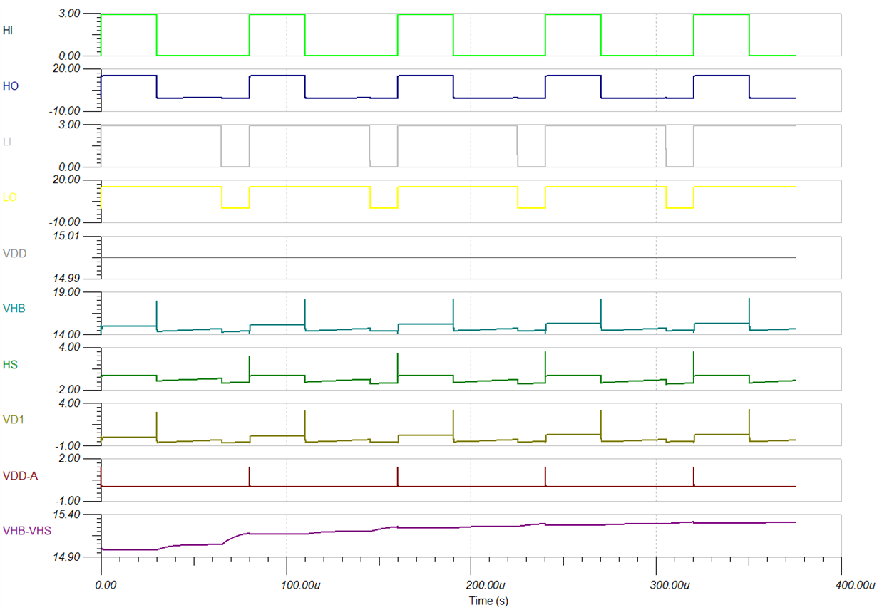
    Please find below updated simulation results after removing IC1:
    Note: Use "Calculate Operating Point" in transient analysis window as mentioned in earlier post.
     
     
    Thanks & Regards,
    Imran
     
  • Hi Imran,

    Never would guess to start simulation COP without ICL0 but no longer need 16v zener on HS. Great find and VDD-A is now producing realistic results.

    Thanks so very much for thoughtful cleverness both you and Arpan!