This thread has been locked.

If you have a related question, please click the "Ask a related question" button in the top right corner. The newly created question will be automatically linked to this question.

DLP3010: DLP3433 DMD bus differential signal P and N are switchable?

Part Number: DLP3010

I am designing projector using DLP3010, DLP3433.

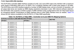
There are DMD bus high speed signals like DMD_HS_WDATA_X_P, DMD_HS_WDATA_X_N.

In my current FPCB design, those signals are crossed. So via is needed in high speed signals.

My question is if HS_WDATA_X_P and HS_WDATA_X_N output can be switchable. Then I can design without via on high speed signals.
If it is possible, please let us know the register address.

  • Hello User,

    In theory, you should not change the DMD interface. We have two software options to support the two different DMD pin mapping options.

    Please refer to the pin mapping options below and you also be able to get more information in the DLPC3433 datasheet

    I hope this helps.

    Regards,

    Lori