


DLP NIRscan™ and DLP NIRscan™ Nano
Table of contents for frequently asked questions on Texas Instruments' spectroscopy evaluation modules.
- Introductory content on Spectroscopy
2. What is the specification of the cuvettes that ship with the DLP NIRScan?
3. I just got my DLP NIRScan Nano. What should I scan?
The DLP NIRScan™ Nano is designed for contact scanning so objects which are flat and uniform make good test subjects. We advise putting the sample in a plastic bag if there is any risk of the sample contaminating the electronics on the spectrometer.
Some have asked if Texas Instruments keeps a database of scans. We do not. However, we do provide some example scans with the TI Design for the DLP NIRScan™ Nano: http://www.ti.com/tool/tida-00554
For a detailed discussion of these issues and some others around getting started with your DLP NIRscan™ Nano, read this thread: https://e2e.ti.com/support/dlp__mems_micro-electro-mechanical_systems/f/983/t/456792#pi319142=1
4. I need information on Sampling Techniques.
To capture the absorption spectrum of a sample, spectrometers commonly used one of these sampling methods:
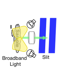
- Transmission sampling consists of directing light through a cuvette or through a NIR transparent material into the slit input of a dispersive spectrometer.
- Transmission sampling is typically used for NIR transparent materials such as liquids, films, oils, fuels, solvent, polymers, plastics, and solutions.
- The main advantage of transmissive systems is that the light is directed through the sample and captured into the input slit of the spectrometer. This provides the most efficient use of light.
![]()
-
- Example of transmissive sampling NIRscan Nano from Optecks:
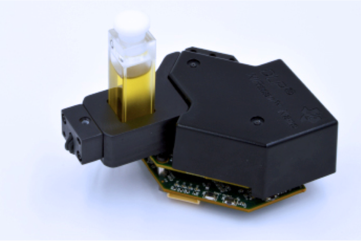
- Example of transmissive sample NIRscan Nano from Young Green:
- Example of a transmission sampling with a light source with fiber output:
- Example of transmissive sampling NIRscan Nano from Optecks:
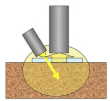
- Reflection sampling consists of shining light into a sample and capturing the reflected light into the input slit of the spectrometer.
- Reflection sampling is typically used for solids, powder, and polymers that are not NIR transparent.
- Reflection sampling typically requires more light power than a transmissive sampling due to the dispersive nature of the sample’s reflection
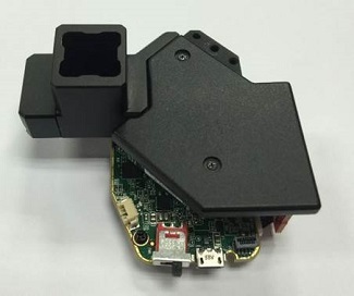
- NIRscan Nano has a reflection sampling head:
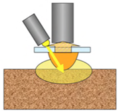
- Transflectance sampling is a combination of the Reflective and Transmissive sample heads. It consists of directing light through the sample and the light is reflected by the background material. Thus, the light passes through the sample twice.
- Transflectance sampling typically is used for liquids, slurries, gels, pastes, polymer. Thin coatings on metal surface also acts as a transflectance system.
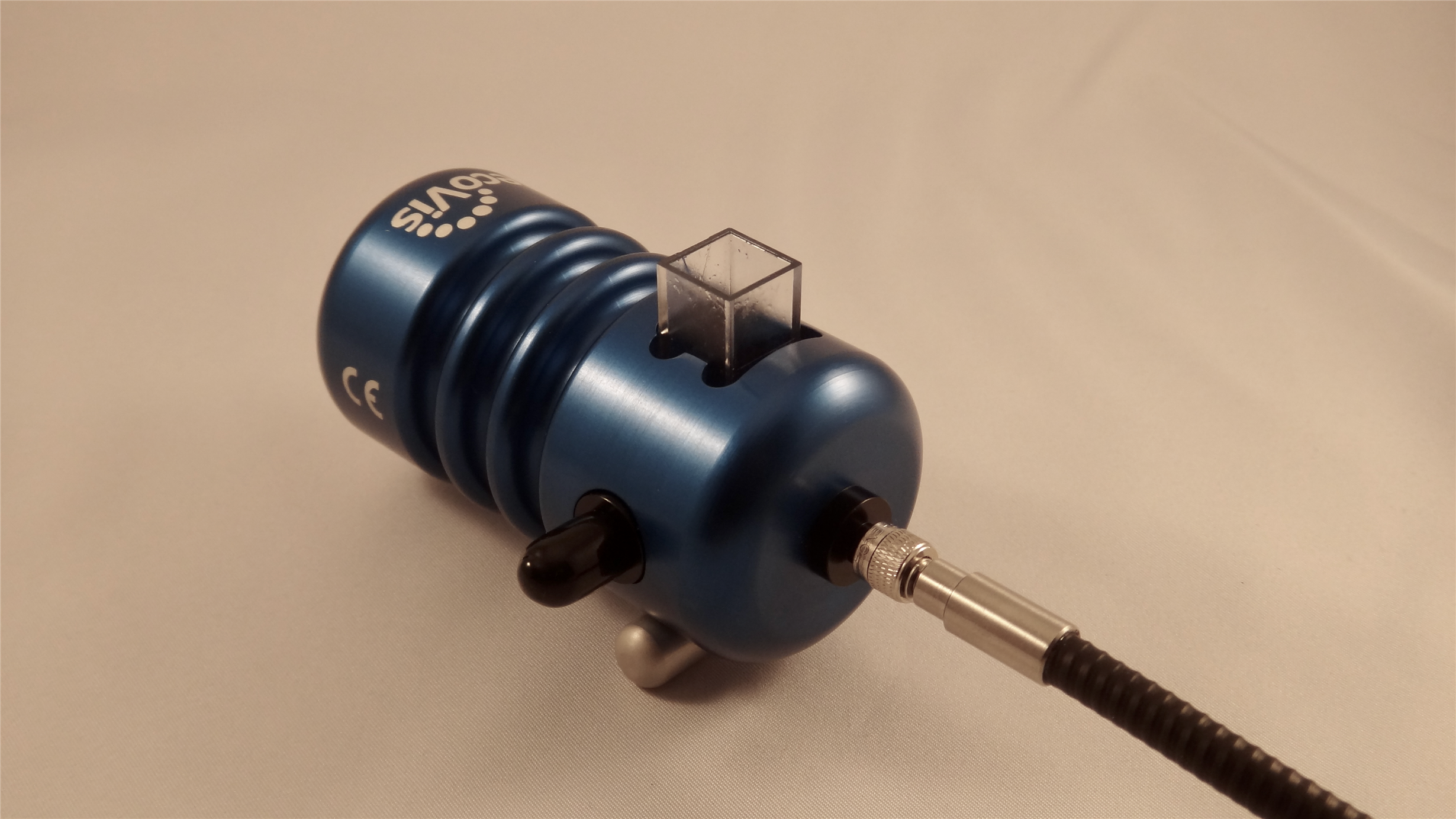
- A popular use of transflectance sampling is in dip probes, where the light is fed through a fiber optic to an open sided probe that has a metal reflective material at the end of the probe.

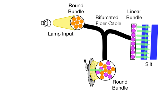
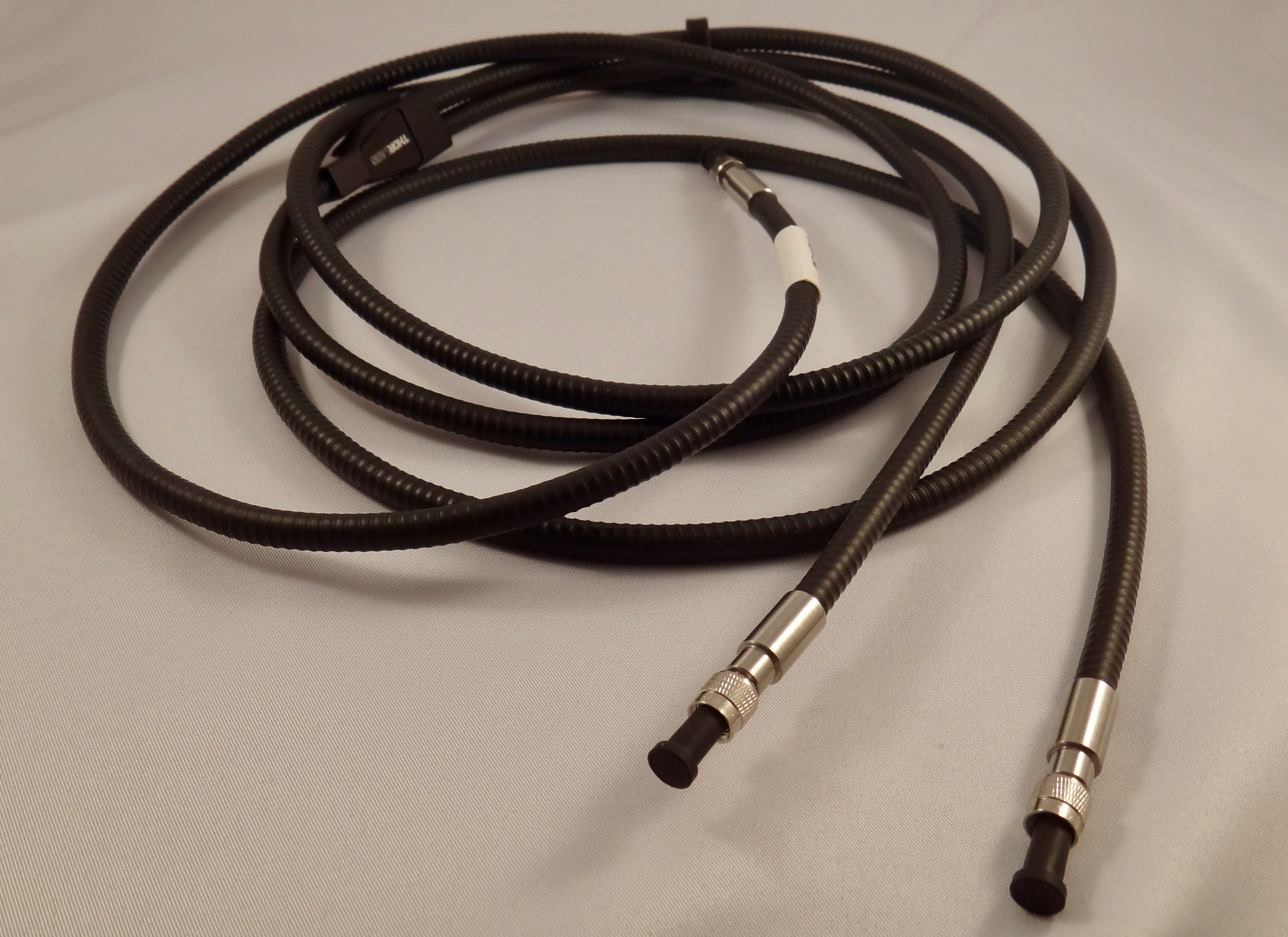
- Fiber optic cable bundles are used in remote sampling. The fiber bundle is typically bifurcated with a set of fiber bundles routed to a light source, while the rest of the fiber bundles capture the reflected light and direct it to the input slit.
- DLP Technology-based spectrometers have tall slits, thus, when combined with round-to-linear fiber bundles that fill the complete slit, the highest performance is obtained:


-
- Sample Preparation
Before taking a scan, samples need to be prepared for consistent presentation. A consistent presentation minimizes sample-to-sample differences and provides a more uniform sample.
Some of the preparations require that:
-
- With liquids:
- The sample is well mixed
- And the sample is poured into a controlled path length, like a cuvette
- With solids:
- Samples might need to be dried to extract excess moisture
- Samples might need to be ground, crushed, pulverized and mixed well to present a uniform consistency
- Samples might also need to be cut or sliced into specific thickness to control the path length
- Samples might also need to be rotated under a scan head to present a uniform consistency. This is typically performed when sampling grain.
- With gases:
- Must be enclosed in a gas cell with sufficient path length to detect the desired compound.
- The gas cell might have a single pass cell or with mirrored walls at end to create an extended path length.
- Temperature and pressure might need to be regulated in the gas cell to contain the gas in a controlled density.b.Contact vs Non-contact Sampling
- With liquids:
Some applications require the avoidance of contact between the sampling head and the system to prevent contamination of the sample or cross-contamination between samples.
There are some major differences between contact and non-contact sampling.
-
- In contact sampling, the light and collection optics are in close contact with the sample. This provide two major advantages:
- First, the reflected light originates mostly from inside the sample and very little from the surface. This spectrum corresponds to the internal composition of the sample and not from the surface.
- Second, the contact sampling provides and captures the maximum light on the sample. The greater amount of light, the greater the signal to noise ratio and the higher performance of the system.
- In contact sampling, the light and collection optics are in close contact with the sample. This provide two major advantages:
-
- In non-contact sampling, the light and collection optics are separated from the sample. This provides:
- Lower light power on the sample since the light power decreases by the distance squared. Therefore, these systems typically use greater lamp power, increasing the power consumption of the system.
- Non-contact sampling provides both the surface composition, and also the internal composition of the sample.
- In non-contact sampling, the light and collection optics are separated from the sample. This provides:

b.Reference Scan
A sample’s absorption of light is measured as the ratio of the light absorbed by the sample and the light incident to the sample. To determine the amount of incident light to the sample, a baseline must be capture. This baseline is referred to as the reference measurement. The NIRscan Nano contains a stored reference measurement in its EEPROM that was created at the factory.
The creation of a reference measurement depends on the sampling method:
-
- For transmission sampling:
- A reference measurement is made by using the same sampling optics, but with no sample present, meaning an empty cuvette.
-
- For a solvent in a solution, the solvent is used as the reference sample.
- For transflectance sampling:
- Non-absorbing surface
- Reference reflective surface in the absence of a sample – if a probe is used, the probe is used without sample as the reference.
- For reflective sampling:
- A broadband and highly reflective NIR coated material replaces the sample. Typical NIR coatings are:
- Spectraflect® from Labsphere
- Gold coated roughened surface.
- A broadband and highly reflective NIR coated material replaces the sample. Typical NIR coatings are:
- For transmission sampling:
This reference measurement must be performed periodically to account for drift due to:
-
- Temperature changes
- Humidity changes
- Lamp intensity variations as lamp ages
- Changes in solvent composition
- Changes in surface reflection during measurement
5. I have questions about the scanning process.
-
- Why do my scans have large dips in an otherwise good curve?
It is possible that when you are scanning you'll get a result like the image shown below. These large dips are caused by the patterns that are used for measuring adjacent wavelengths alternating between two different widths or number of DMD columns used to take the measurement.
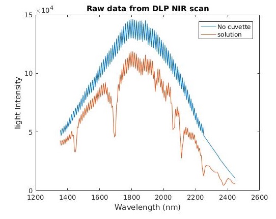
For example, low values might be captured when the pattern is 7 DMD pixels wide, while the higher values might be captured when the pattern is 8 DMD pixels wide. The intensity measured at the detector is proportional to the number of DMD mirrors that are set in the position to reflect incident illumination toward the detector, so as the number of pixels changes in a back and forth manner, the measured intensity will also vary.
More explanation of this effect is available in section 4.2 and figure 9 of the DLP® Spectrometer Design Considerations application note. Specifically, it states:
It is common that the number of columns between the minimum and maximum wavelength to scan is not evenly divisible by the number of wavelength groups desired. In this case, there are a few ways to proceed:
-
-
- Keep the column width constant, and step the on pixel group by an amount different than the column width.
- Change the column width throughout the scan, in order to distribute extra columns
- Enforce a constant column width and step size, allowing only certain numbers of patterns in scans of certain wavelength regions.
-
The DLP NIRscan™ evaluation module uses the second method above. The DLP NIRscan™ Nano uses the first method above. Therefore, the intensity graph of scans performed with the DLP NIRscan™ Nano will not have this behavior.
b.Why do the reported wavelengths differ between two scans defined by the same parameters?
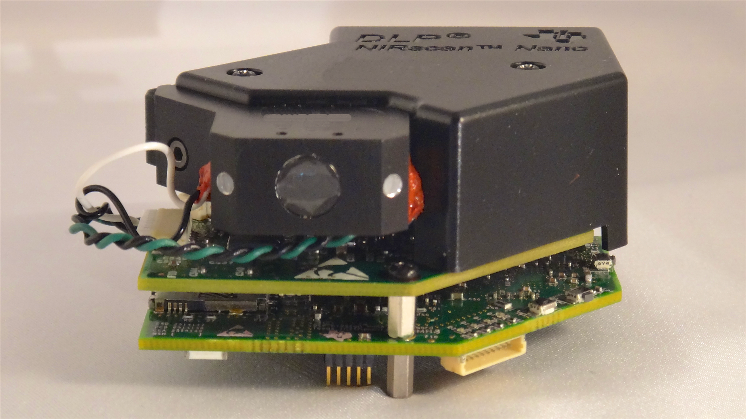
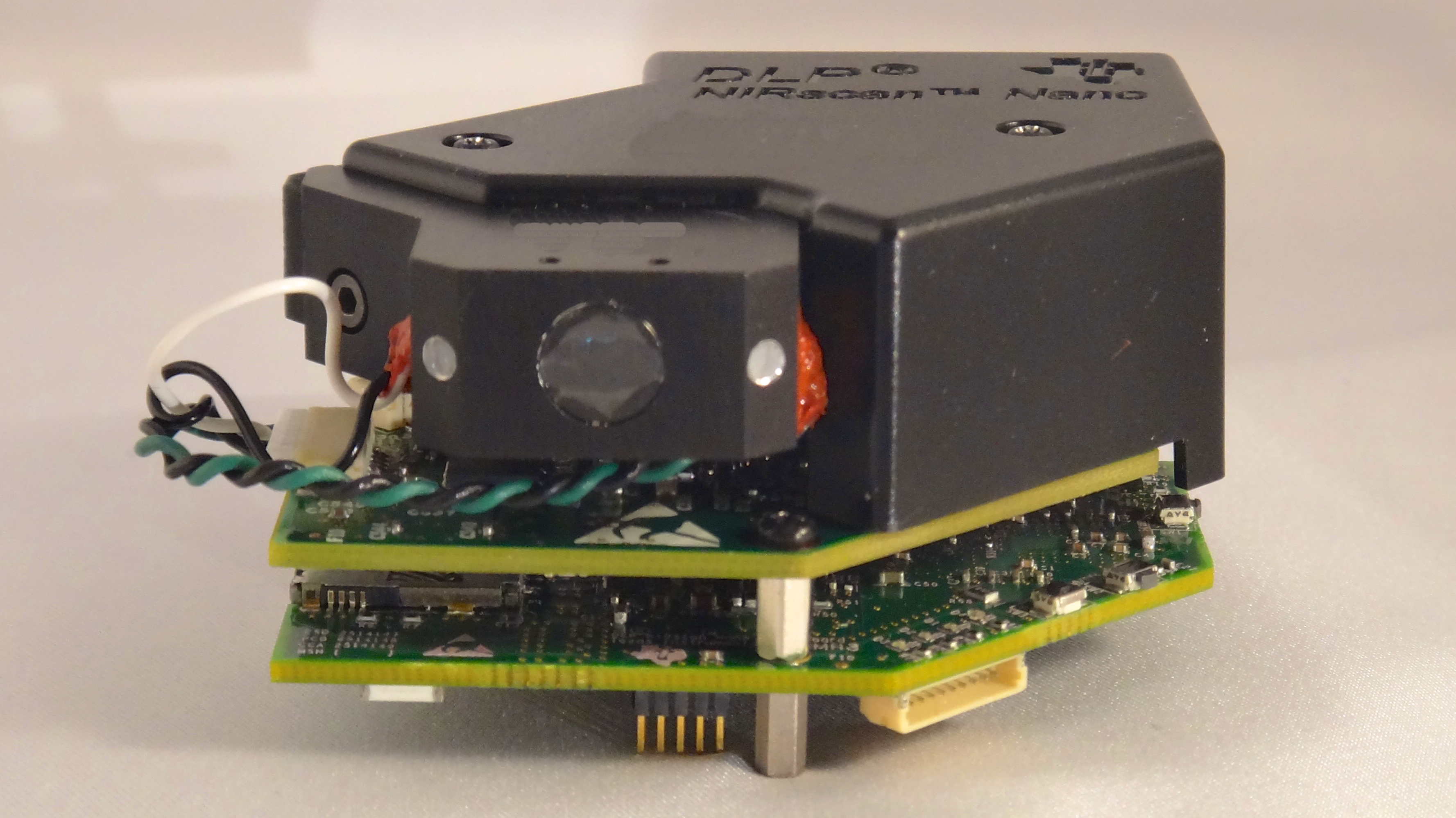
6. I want to know more about the inside of the NIRscan Nano
If you wondered how the DLP NIRscan Nano Evaluation Module (EVM) works, we have disassembled it to show you its internal components and optical paths.
Please note that any disassembly of the optical engine voids the warranty on the NIRscan Nano EVM system and removing the cover on the optical engine allows dust and smudges to collect on the optics affecting its performance. Also, removing the cover might move the optics, slit, and detector out of alignment requiring factory realignment and recalibration. Removing the slit, Indium Gallium Arsenide (InGaAs) detector and DLP2010NIR will require the system to be realigned and recalibrated at the factory.
In short, do not try this at home.
Let’s begin with a quick overview. DLP spectrometers replace the traditional linear array detector with a digital micromirror device (DMD) for wavelength selection and a single point detector. By sequentially turning on a set of columns pertaining to a particular wavelength of light, the light is directed to the detector and captured. By scanning through a set of columns across the DMD, an absorption spectrum can be computed.
DLP technology in Near-Infrared (NIR) spectroscopy provides the following advantages:
-
- Higher performance through the use of a larger single point 1-mm detector in comparison to a linear array with very small pixels.
- Lower cost system through the use of single element detectors and low cost optics. The high resolution DMD allows custom patterns to compensate for the optical distortion of each individual system.
- Greater signal captured not only because of the larger entendue of the DMD compared to traditional technologies, but also through the use of fast, flexible, and programmable patterns and spectral filters.
- With programmable patterns, a DLP spectrometer can:
- Vary the intensity of light to the detector by controlling the number of pixels in a column.
- Vary the resolution of the system by controlling the width of the columns.
- Use a set of Hadamard patterns that capture multiple wavelengths of light per pattern. Individual wavelengths are then retrieved through a decoding procedure. Each pattern turns on 50 percent of the DMD pixel at a time, directing much greater signal into the detector than the column scan shown above.
- Use custom spectral filters to select specific wavelengths of interest.
Currently, DLP NIRscan Nano EVM software supports variable resolution and Hadamard patterns. Variable intensity and custom spectral filters are not supported.
In this picture, you can see the major components of the DLP NIRscan Nano EVM:

Removing the cover to the optical engine reveals the DMD and Detector board:
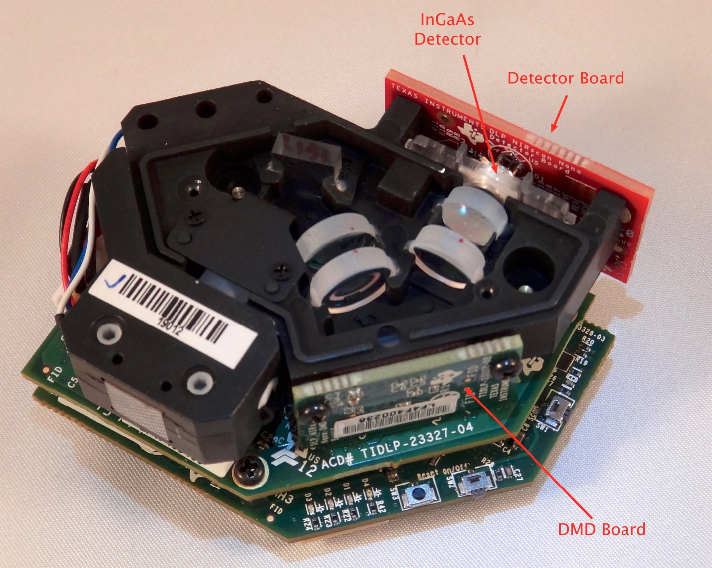
Now if we removed the Reflectance module, you can see the slit:
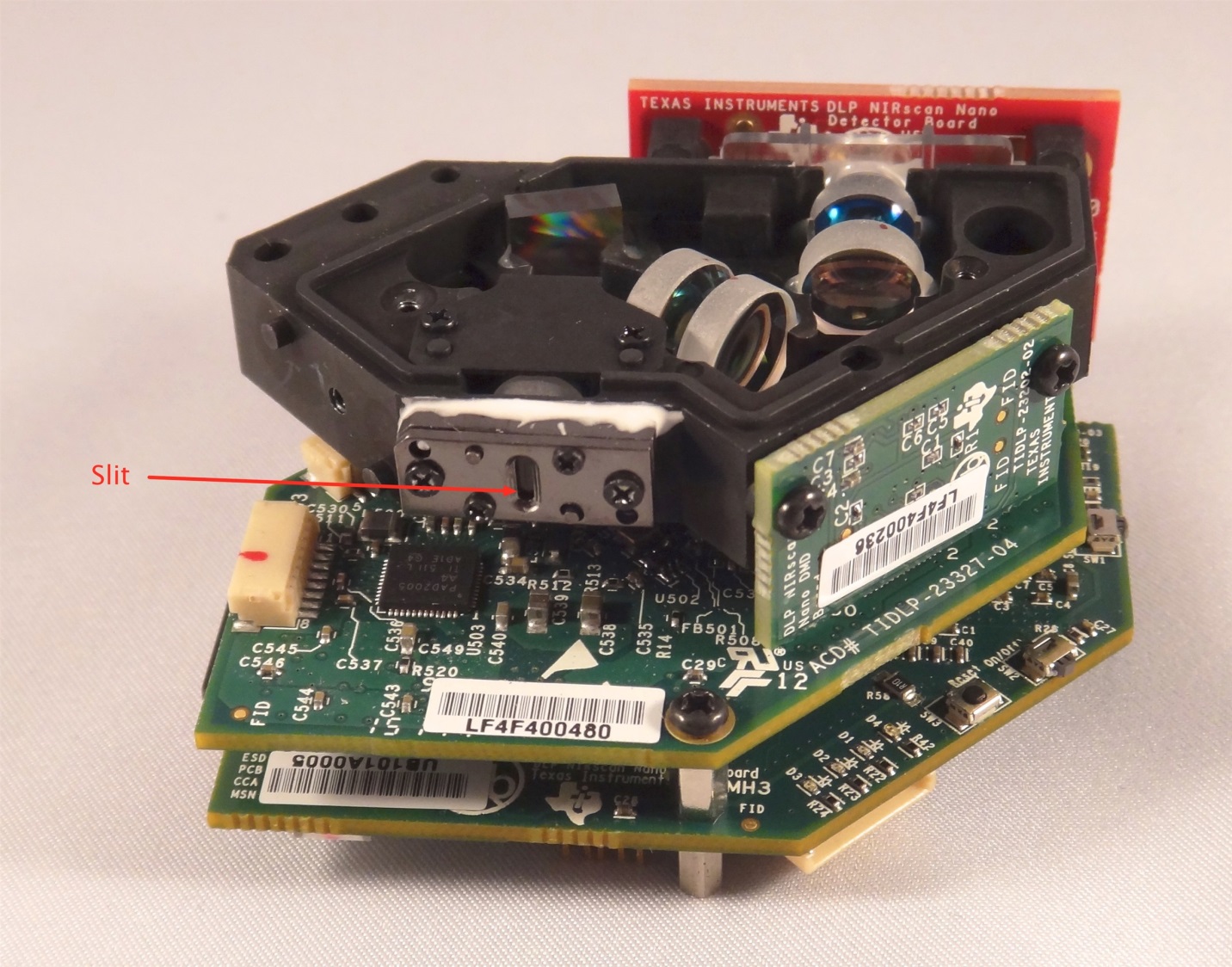
Now that we’ve gotten inside, let’s take a look at how the light is manipulated.
The light reflected from the sample is gathered by the Collection lens and focused into the optical engine through the input slit. The slit size is chosen to balance wavelength resolution with signal-to-noise ratio (SNR) of the spectrometer. This spectrometer uses a 25 μm wide by 1.69 mm tall slit. The light that passes through the slit is collimated by the first set of lenses, passes through an 885-nm long wavepass filter, and then strikes a reflective grating. This grating, in combination with the focusing lens, disperses the light into its constituent wavelengths (multi-colored light rays). The focusing lenses form an image of the slit at the DLP2010NIR DMD. Different wavelengths of this slit image are spread horizontally across the DLP2010NIR DMD. The optical system images 900 nm wavelengths to one end of the DMD and 1700 nm to the other end, with all other wavelengths sequentially dispersed in between.

For more information on DLP NIRscan Nano EVM, refer to the DLP NIRscan Nano User’s Guide.
7. Where can I find more documentation on developing a DLP technology-based spectrometer?
The following TI documentation provides further information on developing a DLP technology-based spectrometer:
-
- DLP Technology for Spectroscopy (DLPA048)
- DLP Spectrometer Design Considerations (DLPA049)
- DLP NIRscan Nano Evaluation Module (EVM) Optical Design Considerations (DLPA062)
- Flexible Trade-offs in Maximizing SNR and Resolution in TI DLP Technology Based Spectrometer System (DLPA066)
- Signal Chain Performance Optimizations in the TI DLP® Technology-Based Spectrometer (DLPA072)
The following reference designs are available:
- DLP Ultra-mobile NIR Spectrometer for Portable Chemical Analysis with Bluetooth Connectivity
- Illumination
- Opto-Mechanical
- Board Files
- Bill of Materials (BOM)
- Schematics
- Board Layout Files
- Gerber Files
- PCB Files
- DLP Near-Infrared Spectrometer for Optical Analysis of Liquids & Solids Reference Design
The following User's Guides are available:
The following videos are available:
- TI DLP technology for mobile NIR sensing
- Getting started with the DLP NIRscan Nano
- DLP NIRscan Nano design considerations
- DLP NIRscan design considerations
The following DLP technical documents are available:
8. Can I change the resolution and wavelength range of DLP NIRscan and DLP NIRscan Nano?
The optical architecture of the DLP NIRscan and DLP NIRscan Nano can accommodate various resolution and wavelength ranges with minor changes to the optical layout.
- Changing resolution:
- The resolution of the system is dependent on the convolution of the slit width, optical point spread function, and DMD pattern width. As pattern and slit width decreases, less light reaches the detector. This leads to some tradeoffs between SNR and resolution. Refer to the Flexible Trade-offs in Maximizing SNR and Resolution in TI DLP® Technology-Based Spectrometer Systems Application Report for detailed information on these tradeoffs between SNR and resolution with different slit and pattern widths.
- Changing wavelength range or bandwidth:
- The wavelength range or bandwidth is dependent on the grating's groove spacing and the distance between focusing lens and grating. For the same grating and focusing lens, the farther the lens to the grating, the smaller the wavelength range. The smaller wavelength range allows for finer resolution at the same slit and pattern width. Note that the slit is imaged onto the DMD, so changing the distance of the DMD to the grating requires changes to the focusing lenses and their spacing. The DLP NIRscan has a wavelength range of 1100 nm while the DLP NIRscan Nano has a wavelength range of 800 nm.
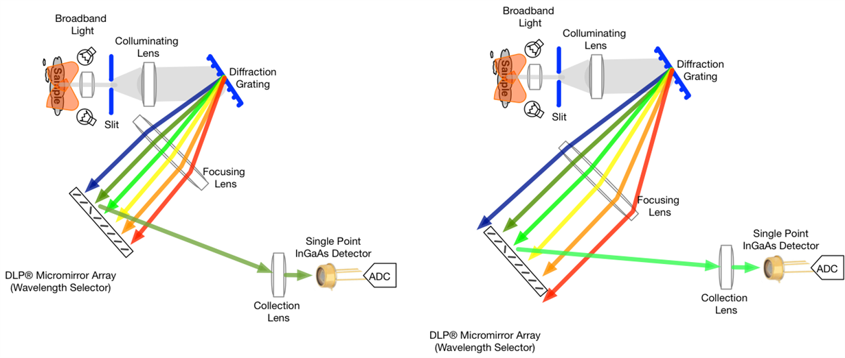
- The wavelength range or bandwidth is dependent on the grating's groove spacing and the distance between focusing lens and grating. For the same grating and focusing lens, the farther the lens to the grating, the smaller the wavelength range. The smaller wavelength range allows for finer resolution at the same slit and pattern width. Note that the slit is imaged onto the DMD, so changing the distance of the DMD to the grating requires changes to the focusing lenses and their spacing. The DLP NIRscan has a wavelength range of 1100 nm while the DLP NIRscan Nano has a wavelength range of 800 nm.
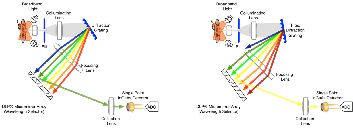
- Shifting the wavelength range:
- The tilt of the grating dictates the set of wavelengths that fall on the DMD's active area. Tilting the grating shifts the wavelength range of the system. In the DLP NIRscan Nano a few degrees of tilt on the grating would change the wavelength range of 900 - 1700nm to 1100-1900nm. This will not change the wavelength range of the system, just shift the start and end wavelength points. Since the slit is imaged onto the DMD, the slit position must be adjusted to refocus all the wavelengths at the DMD with the change in the grating tilt. The grating tilt is not inherently adjustable in the NIRscan Nano, and will require some physical modification of the chassis around the grating.
- The DLP NIRscan and DLP NIRscan Nano have InGaAs photodetectors optimized for a specific wavelength range. Thus, shifting the wavelength range requires replacing the photodetectors to support the new wavelength range. For example, the DLP NIRscan Nano's photodetector sensitivity rolls off sharply at 1700nm, so a system supporting 1100-1900nm would need to be replaced with an extended range detector that is sensitive to 1900nm. Refer to Signal Chain Performance Optimizations in the TI DLP® Technology-Based Spectrometer Application Report for examples of extended range photodetectors and the appropriate transimpedance amplifier considerations. During production of the EVM, the detector is also flown in place on an x-y-z translation stage to maximize received signal, and then glued in place. Replacing the photodetector requires the alignment process to be repeated and potentially moving the condenser lens position to accommodate the new detector.
- The following efficiency losses might require more powerful illumination sources to counteract the lowered system throughput. The efficiency loss depends on the new wavelength range and sensitivity of the new detector.
- The blazed diffraction grating efficiency decreases when it is used at wavelengths farther from its nominal blaze wavelength.
- The lenses anti-reflective (AR) coatings are less effective at longer wavelengths. The lens glass absorption increases noticeably past 2000nm.
- The diffraction efficiency of the DMD may decrease at the longer wavelengths.
- Extended photodetector sensitivity tends to be lower than the non-extended photodetectors.
- When simulating the new optical design to determine the appropriate grating tilt angle, ensure that the wavelengths of interest are not being vignetted at the edge of the DMD. Keep in mind that mechanical tolerance stackup can cause small shifts in the wavelength position at the DMD. The amount of margin necessary between the measurement wavelengths and the edge of the DMD array will vary based on the accuracy of the grating tilt adjustment.
- It will also be necessary to replace the long wavelength pass filter that is located between the collimating lenses and the diffraction grating. For example, in the DLP NIRscan Nano, this filter blocks light below 900nm from reaching the grating in order to prevent stray light from the second diffraction orders of short wavelength light reaching the DMD. A new filter with a cutoff appropriate for the shifted measurement spectrum should be used.
- Modifications to the chassis are necessary to allow for grating tilt and the potential movement of condenser lens to accommodate the new detector.
- Finally, end calibration will be dependent on the calibration sources chosen for your target wavelength range. For example in the DLP NIRscan Nano, the GUI software needs to be modified to calibrate for the shifted wavelength range, since it is currently optimized to calibrate a 900-1700nm instrument.
- The tilt of the grating dictates the set of wavelengths that fall on the DMD's active area. Tilting the grating shifts the wavelength range of the system. In the DLP NIRscan Nano a few degrees of tilt on the grating would change the wavelength range of 900 - 1700nm to 1100-1900nm. This will not change the wavelength range of the system, just shift the start and end wavelength points. Since the slit is imaged onto the DMD, the slit position must be adjusted to refocus all the wavelengths at the DMD with the change in the grating tilt. The grating tilt is not inherently adjustable in the NIRscan Nano, and will require some physical modification of the chassis around the grating.

9. Compiling and modifying Tiva software
-
- Required Tools to Compile Tiva Software
- Code Composer Studio (CCS) Integrated Development Environment (IDE) version 6.0.1 (Windows, Linux, and macOS versions)
- TI-RTOS for TivaC version 2.10.1.38
- OptionalTools for software debugging
- XDS200 Emulator with TI 20-pin to ARM 10-pin converter adapter
- Download Software
- NIRscan Nano Tiva Sources, you will need a Windows PC run the installer and extract the files.
- DLP Spectrum Library Sources, you will need a Windows PC run the installer and extract the files
- Compiling required libraries
- To compile the TivaWare driverlib library, follow these steps:
- Import the driverlib library by selecting Import from the File Menu.
- In the new Import dialog window, select CCS Projects under C/C++ folder and click Next.
- Find the location of the TivaWare driverlib project by browsing to the directory
C:\ti\tirtos_tivac_2_10_01_38\products\TivaWare_C_Series-2.1.0.12573c\driverlib and click OK.
- Import the usblib library by selecting Import from the File Menu.
- In the new Import dialog window, select CCS Projects under C/C++ folder and click next.
- Find the location of the TivaWare usblib project by browsing to the directory
C:\ti\tirtos_tivac_2_10_01_38\products\TivaWare_C_Series-2.1.0.12573c\usblib and then click OK. - Compile this newly added usblib project by select Clean from the Project Menu. Ensure that usblib project is checked and select "Build only the selected project" and then click OK.
- To compile the TivaWare driverlib library, follow these steps:
- The DLP Spectrum Library is a collection of C-language routines that provide the fundamental pieces to use a DLP system in a spectroscopy application. These routines are shared by the Tiva firmware, NIRscan Nano GUI, and iOS App. To compile the DLP Spectrum Library for Tiva firmware, follow these steps:
- Import the DLP Spectrum Library by selecting Import from the File Menu.
- In the new Import dialog window, select CCS Projects under C/C++ folder and click Next.
- Find the location of the dlpspeclib project by browsing to the install directory: C:/ti/DLPNIRNANO_SPECLIB.
- Compile this newly added dlpspeclib project by selecting Clean from the Project Menu. Ensure that dlpspeclib project is checked and select "Build only the selected project" and then click OK.
- The Tiva main program sources are installed by the DLPNIRscanNanoSoftware package. This package installs the Code Composer Studio project and source at the default directory C:\ti\DLPNIRscanNanoSoftware_vX.X.X
- Import the Mobile Spectroscopy Tiva EVM by pulling-down the File Menu and select Import.
- In the new Import dialog window, select CCS Projects under C/C++ folder and click Next.
- Find the location of the Mobile Spectroscopy Tiva EVM by browsing to the install directory of the sources: C:\ti\DLPNIRscanNanoSoftware_X.X.X\Sources.
- Make sure all the other libraries are compiled and imported before this step. Then, compile this newly added Mobile Spectroscopy Tiva EVM project by selecting Clean from the Project Menu. Ensure that dlpspeclib project is checked and select "Build only the selected project" and then click OK.
- Required Tools to Compile Tiva Software
- Reconfigurable compile options:
- The Tiva firmware can be recompiled to map the buttons and LEDs to the expansion connector J3. The following #defines control how these buttons are mapped. These are set in C:\ti\DLPNIRscanNanoSoftware_2.0.1\Sources\App\include\common.h
-
- Compiler switch to remap Scan button input from Expansion Connector J3 pin 8 = SCAN_BUTTON_EXP_CONN
- Example to remap the scan button to Expansion Connector J3 pin 8, change line 195 from
/*** Compiler switch to remap Scan button** 0 = Scan button input from Expansion Connector J3 pin 8* 1 = Scan button input from Scan button on Tiva Board*/#if 1#define SCAN_BUTTON_TIVA_BOARD // PQ3#undef SCAN_BUTTON_EXP_CONN#else#undef SCAN_BUTTON_TIVA_BOARD // PK3#define SCAN_BUTTON_EXP_CONN#endif
to:
-
-
- Compiler switch to remap GREEN LED output to Expansion Connector J3 pin 6 = GREEN_LED_EXP_CONN
- Compiler switch to remap YELLOW LED output to Expansion Connector J3 pin 3 = YELLOW_LED_EXP_CONN
- Compiler switch to remap BLUE LED output to Expansion Connector J3 pin 7 = BLUE_LED_EXP_CONN
-
-
- The Tiva firmware can be recompiled to have Bluetooth advertising at startup
- Compiler switch to enable BLE advertsing at startup = ENABLE_BLE_AT_STARTUP
- Example to enable BLE advertising, change line 171 from:
- The Tiva firmware can be recompiled to have Bluetooth advertising at startup
/**
* Compiler switch to enable BLE advertsing at startup
*/
