Other Parts Discussed in Thread: DS160PR410
Hi
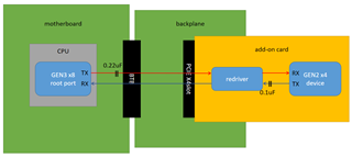
The picture below is my block diagram. I am designing a PCIe add-on card with FR4 4-layer PCB.
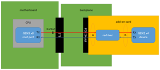
The entire system has 0.22uF capacitors on the CPU TX side, and the root port can support GEN3 X8 signals, while the end device on my add-on card only supports GEN2 X4 signals.
I want to use DS50PCI401 for my add-on card.
I didn't see any layout suggestions on the datasheet.
1. I want to know if there is a layout guide for DS50PCI401?
2. In my picture, do I need any capacitors on the TX or RX side of node A (between the PCIe slot and the redriver)? If capacitors are needed, what value is recommended?
3. In my picture, do I need any capacitors on the TX or RX side of node B (between the redriver and the device)? If capacitors are needed, what value is recommended?
4. At node A (between the PCIe slot and the redriver), what is the minimum and maximum limit of the trace length?
5. At node B (between the redriver and the device), what is the minimum and maximum limit of the trace length?
6. Where is the recommended location for the redriver? Near the device or the slot? Because the size of my add-on card is not very large, may the placement position be unimportant?
7. According to the data sheet, there are many hardware pins that can be set, such as EQ level, de-emphasis level, etc. I want to know if I want to set High level to 1 or Low level to 0, what is the value of the resistor PU? Or PD?
8.Are there any important layout suggestions that need attention?
Thank you very much.