This thread has been locked.

If you have a related question, please click the "Ask a related question" button in the top right corner. The newly created question will be automatically linked to this question.

DS80PCI800: location of AC coupling capacitor ?

Genius 3870 points
Part Number: DS80PCI800

Hi there,

When layout PCIe3.0 , the location of AC caps often confused me. I searched through this forum, found various answers based on different experience. 

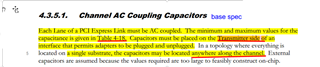
I looked into PCIe base spec(pic below), the are two situations defined:

(1) Both TX and RX chips are on same board, the spec claimes AC cap can be located ANYWHERE along the channel. Not sure whether this is correct, as I see most real design placed the caps as close as possible to TX or RX chip. 

(2) The plug-in card architecture, TX and RX chips are on different boards, connector exists.  The spec only requires AC cap be placed on TX side, I assume this is not enough. Should caps be close to TX chip or the connector? As I see most real design (like some commercial PC motherboard) the AC caps are usually placed near the CONNECTOR. Do not understand why. I think close to chip would be better for signal integrity.

Appreciate if some expert could help explain in detials. Thanks !

  • Greetings,

    1). When both TX and RX chips are on the same board, it is recommended to put the AC coupling Cap as close to the RX as possible. This is because RX ESD structure creates an impedance drop. AC coupling Cap pads cause impedance drop as well but typically not ass much as the ESD structure of the receiver. So putting the Cap close to the RX would causes the impedance drop due to Cap to be swamped or it is negligible with respect to the ESD impedance drop.

    2). When there is a PCIe plug in Card, it is recommended to place the Cap on the TX side and close to the connector - mainly for the same reason as noted in #1 above.

    Regards ,, Nasser

  • Hi Nasser, 

    you mentioned "putting the Cap close to the RX would causes the impedance drop due to Cap to be swamped or it is negligible with respect to the (RX's) ESD impedance drop / connector impedance drop",   

    my qualitative understanding to this sentence is as below, just to confirm I did not misunderstood your meaning: 

    AC cap, RX ESD structure, and connectors can all be seen as Discontinued Impedance Points along the PCB trace. If they are placed CLOSE ENOUGH, the Impedance  drop caused by AC cap(smaller) and RX ESD structure(larger) could be approximately seen as ONE Discontinued Impedance Point, so this is better for signal integrity. 

    By the way, I think you answer applied to general situation including but not limited to DS80PCI800. 

    Thanks again.

  • Greetings,

    Your understanding is correct.

    Regards ,, Nasser