This thread has been locked.

If you have a related question, please click the "Ask a related question" button in the top right corner. The newly created question will be automatically linked to this question.

DS125BR401: Expected output eye-diagram for PCIe link with DS125BR401SQE IC

Part Number: DS125BR401

Hi,

In our design, we have used Jetson NX as Root Complex and Arria 10 FPGA SoC board as End Point configuration.

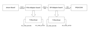
Hardware configurations (boot strapping) for, PCIe generation 2, x2 (lane 0 and lane1), the repeater is as follow,

Equalization=0x02, for FR4 10-inch trace,

De-emphasis=-3.5dB,

VOD=0.9V.

Link is stable and communication between boards is working fine.

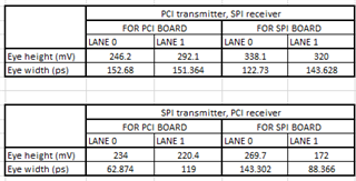
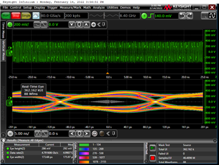
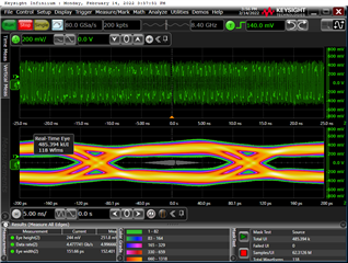
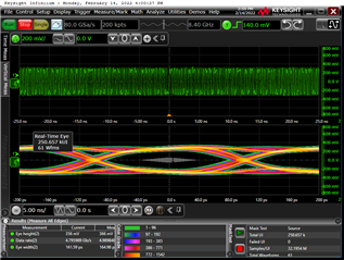
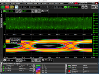
Results captured before and after repeater IC for lane 0, where Jetson kit is transmitting and FPGA is receiving, as per bring-up test are as follow

On PCI board, before repeater IC:

On PCI board, after repeater IC:

On SPI board, before repeater IC:

On SPI board, after repeater IC:

We’re getting similar results when communication is inversed and on lane 1 as well in both situations.


I wanted to know that if eye-diagram captured are as expected or not, and why eye is bulged after, and it is more accurate before repeater. If yes, what is the technical reason behind such behaviour?

Moreover, as you can see in block diagram we have two adaptor boards, PCIe and SPI, and we’re not getting same type of eye behaviour at, after repeater on PCIe board and before repeater on SPI board.

Thanks, 

Zeel Shah

  • Hi Zeel,

    Moreover, as you can see in block diagram we have two adaptor boards, PCIe and SPI, and we’re not getting same type of eye behaviour at, after repeater on PCIe board and before repeater on SPI board.

    Can you clarify, does the output signal from the DS125BR401 on the PCIe board feed into the input of the DS125BR401 on the SPI board?

    Thanks,

    Drew

  • Hi Drew,

    Yes, output signal from the DS125BR401SQE on the PCIe board is fed to the input of the DS125BR401SQE on the SPI board.

    Thanks,

    Zeel

  • Hi Zeel,

    I believe the reason you are seeing the bulge after the redriver on the PCIe board is that this signal is over equalized at the point it is measured.  This is necessary to have a properly equalized signal at the input to the redriver on the SPI board.  Your measurements seem to confirm that this is the case since the input to the redriver on the SPI board looks appropriately equalized.

    Thanks,

    Drew

  • Hi Drew,

    Thanks for your response. Do you mean to say that the HW equalization on PCIe board is more than what it should be?

    We have tried multiple values of equalization on PCIe board and the current values are the only ones in which we always get the PCIe link detected and so this is chosen. We do not get stable PCIe link in any other values.

    Let me know if I need to clarify this point further. Please guide on what should be the next step to fine tune this.

  • Hi Zeel,

    To clarify my previous response, I was claiming that the bulge and jitter observed in the eye diagram labeled "On PCI board, after repeater IC" are expected.  This is because the redriver is currently tuned to create a well conditioned signal at the eye diagram labeled "On SPI board, before repeater IC".  In order to compensate for the loss between the PCIe and SPI board, the redriver is on the PCIe board equalizes the signal to be well conditioned at the "On SPI board, before repeater IC" location in the system, which means that the signal will appear over-equalized at the "On PCI board, after repeater IC" location.  This is expected.

    Based on my current understanding of your system, I do not see any issues with the eye diagrams you have attached.  If your system is stable with these equalization settings, then I believe they are appropriate.

    Thanks,
    Drew

  • Hi Drew,

    Understood your point, thanks for the clarification. It explains the eye-diagram captured and are in accordance with our results as well however, I have one query.

    I’ve attached the results captured, after the re-driver on both, PCIe and SPI, boards and it provides quite a margin but there is difference in values for both boards which might be due to designing and layout variations in both boards.

    (Note: Values mentioned are mean values for the samples captured)

    As of now, we’re testing with single board before transmitting signal, but customer is planning to extent it further, i.e., using multiple boards before signal is transmitted from PCIe to SPI board or vice versa, which may result into more discontinuities resulting into more impedance mismatch that might cause distortion in input signal fed to the redriver.

    So, is there any provision of adaptive equalizing with this redriver which can sense the input values and choose the values of equalization, de-emphasis, and VOD accordingly to get better output, in case of distorted input. If not by hardware strapping, then by SMBus mode or other ways.

    Thanks,

    Zeel

  • Hi Zeel,

    Unfortunately this part does not have any adaptive equalization capabilities.  Some of our retimes have adaptive equalization, but unfortunately we do not have a retimer for PCIe available.

    In regards to your eye data, I see that one of the measurements has an eye height that is significantly smaller than the others (172mV vs >200mV).  Is there any difference in the signal paths that might account for this, or is this just a result of manufacturing variance?

    Thanks,

    Drew

  • Hi Drew,

    There could be some measurement variance but manufacturing variances are less probable.

    I wanted to know what should be the approximate values/range if there are no delta in terms of manufacturing or measurement errors.

    Thanks, 

    Zeel

  • Hi Zeel,

    I will have to look into this and get back to you.

    Thanks,

    Drew

  • Hi Zeel,

    I would expect a 10-20 mV variation in eye height between redrivers, assuming all other factors are held constant.

    Thanks,

    Drew