This thread has been locked.

If you have a related question, please click the "Ask a related question" button in the top right corner. The newly created question will be automatically linked to this question.

TPS65983B: Titan-Ridge DD - Tapex Creek FW config

Part Number: TPS65983B

Dear TI team:

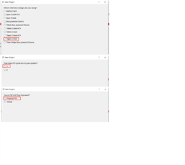
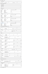
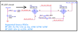
We are currently developing a TBT3 Titan-Ridge DD project, and the PD chip used is TPS95683B used on the reference version. I am not sure about the configuration of FW. Attached is our schematic diagram for your reference.

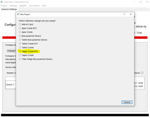
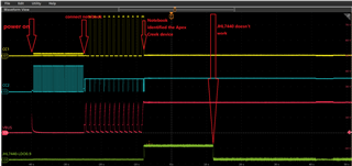
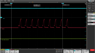
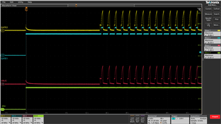
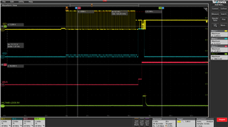
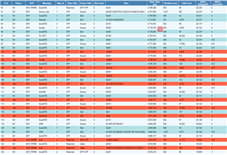
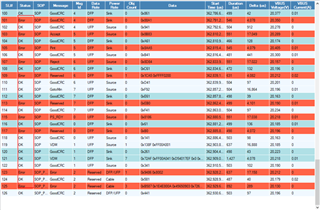
We need type-c to output 5V@3A,9V@3A,15V@3A,20V@3.25A through ATX power supply, but could you please help to confirm the specific FW configuration? The attached screenshot shows the FW configuration.

Tanks!

tbt3_card_V10.pdf

  • Hello,

    The individual that would be able to best assist with this question is currently out of the office, but will return next week. Apologies for the delay.

  • Thank you for your reply. I look forward to hearing from you. Thank you!

  • In the meantime, one question I have is the reason for not wanting to implement TBT4/USB4? Since you are following an Intel reference design, curious the reason for not implementing the latest reference design. Since the release of Intel's TBT4/USB4 controller, I have not seen too many questions about Titan Ridge and the TPS65983B

  • Tr-DD is more suitable for our product requirements, so we chose TR-DD as a reference.

  • Thank you for the clarification. 

  • Is there any update?

  • Hi Xiang,

    The engineer is still out of office but I will be sure to get back to you as soon as I can get with him. Thanks for your patience.

    Regards,

    Taylor

  • Hi Team,

    For any ATX application the reference design must be followed exactly. If you are using the Tapex Creek ATX version select the project below. If you are using a single port set the 1 port option and most likely you will need to do virtual DP Hot Plug Detect.

    Jacob

  • Could you check the schematic for me, please?

    I have two questions.

    1. Do CC1 and CC2 have to be high impedance or grounded in the case of external power input?

    2. The reference line controls 9V or 15V output through GPIO5 and GPIO6. The default is 5V, but our line defaults to 20V,Would that be a problem?

  • Hi Xiang,

    As Jacob mentioned above, the reference design must be followed as is for this project. Otherwise it may be possible if you have a TI FAE contact, they can work to submit an official review internally. 

    1) The CC pins are designed to be connected to the type C connector or through a protection device and will handle all the required impedance control automatically.

    2) The reference design must be followed exactly as is, otherwise it may cause issues.

    Regards,

    Taylor

  • We have followed the reference design.

    However, the problem is that PD's RST signal will be sent when host is not connected, but PD's RST signal will not be sent when host is connected. May I ask what is the problem?

  • Xiang,

    Can you clarify what you mean by PD's RST signal? Which signal or pin exactly (for example HRESET/RESETZ?)? Can you capture the signal and send it?

    If RESETZ issue, then please check VOUT_3V3 is expected high when the core is powered. RESETZ is an active low reset output when VOUT_3V3 is low. 

    Regards,

    Taylor 

  • Now the RESETZ signal is fine. When I plug in the host(Notebook), RESETZ will output a high signal to the TR main control IC.

    In the FW configuration, register 0x32 I choose four power supplies,5V,9V,15V,20 which I can understand.

    But how can I edit the values of registers 0x44 and 0x47?

    0x47: How to fill in the ID value? As explained in the video tutorial, the value of this register is related to authentication only and does not affect functionality. In my experiment, I found that changing different ID values, thunderbolt devices and USB devices could be recognized under Windows.

    0x44: Peak Current 1, 2, 3 Are these values required? What are the rules for filling in? How to fill in source Input, Touch Current, compliant and other parameters?

    Attached is the FW file prepared by myself. Could you please help me check it?1258.TPS65983B_fw6_Intel_Tapex_Creek_Static_1port_v4_14.rar

  • Xiang,

    As said previously and in the below thread, the settings must stay the same as in the default configuration file in the instructions above so we are not able to review a new config file. If you are altering settings, you may run into issues for this design.

    https://e2e.ti.com/support/interface-group/interface/f/interface-forum/885632/tps65983b-tps65983b-i2c-address-setting-question-in-tapex-creek-platform

    Regards,

    Taylor

  • Sorry for the late reply.

    The current situation is that I use the default FW Settings and then burn them into the Intel FW file, but there is a problem: PD can switch different voltages to the VBUS of USB-C when connected to different devices. But the main control JHL7440 is still not working. Why?

    Intel's FAE says the timing and working mode of the master chip are controlled by PD, but the JHL7440 still doesn't work, and the Thunderbolt device can't be identified when connected to the Notebook. What kind of question is that?

    The design of the hardware has been based on Intel design.

  • Xiang,

    You mention the design is 'based' on the Intel reference but to be clear, it needs to be identical from hardware and the firmware settings perspective. Please check these match. Otherwise you will need to take logs of the messaging to the JHL7440 to figure out what settings may have caused incorrect behavior.

    Regards,

    Taylor

  • Dear Taylor,

    I'm sorry I had a problem with my description.

    The current hardware design is completely consistent with the Intel reference design.

    The FW config also uses the default Settings.

    Regards.

  • Xiang,

    Ok but in the initial question above, you had changed the FW settings for review, so please be sure you did not change them from the default GUI template for Tapex Creek. If that is the case that it is still not working then I recommend collecting any PD logs and I2C commands especially between the JHL device and our PD controller so we can see what may be going on.

    Regards,

    Taylor

  • Dear taylor:

    I have measured that the input of 65983B VIN_3V3 has 3.3V voltage. Both VOUT_3V3 and LDO_3V3 have 3.3V, LDO_1V8D and LDO_1V8A have 1.8V.

    The attachment is cc communication log and I2C log. I am responsible for hardware engineer, but I am not familiar with software. Please let me know if you have any questions, thank you!

    Regards.65983B-log.rar

  • Hi Xiang,

    What program do I need to open this type of older I2C log file?  Can you link the download?

    As for the PD log, what are you attempting to do here? It seems like some cable disconnects and then some errors - what is the goal on turn on and is our PD controller in this case the DFP or UFP?

    Thanks,

    Taylor

  • Dear Taylor:

    I have saved I2C logs in CSV, TXT and bin formats. Would you please see which format you can open?

    As for PD's log, I did not disconnect the cable during the whole recording process. The expansion dock connects to the Notebook and charges it. In this case, the PD controller on the expansion dock should be DFP.

    Regards

    TPS65983B-I2C-LOG-20220329.rar

  • Xiang,

    It is typically easier to view the log in the program you captured it (like for Saleae there is a logic program), can you identify the program you captured the .kvdat file with?

    As for the pd log it does seem things start to error out after a number of back to back Good CRC commands. Can you send your updated config file you are using to confirm it matches the Tapex creek recommendations?

    Thanks,

    Taylor

  • Dear Taylor:

    Kingstvis_v3.5.3. rar This is the software I used to capture I2C logs, you can view I2C(.kvdat) logs through this software.

    Pd-0328-1.rar This is the PD FW file I am using.

    Regards

    software or PDFW.rar

  • Update:

    I did the experiment again, and the process was as follows:

    1) : After connecting to the Notebook, wait for a while and the Notebook will recognize the Tapex Creek device as shown below.

    2) : At the same time, the Notebook starts slow charging (The Notebook supports 100W charging, and the maximum power of 65983B is 85W). At this time, the main control chip JHL7440 will have an internal 0.9V voltage output and crystal oscillator will work.

    3) : After a while, the internal 0.9V shuts down and JHL7440 does not work.

    I have attached PD log and I2C log of this whole process, please check.

    I didn't connect to any device and only connected to the Notebook through usB-C.

    Can you tell what the problem is from the log?

    TPS65983B-20220331-LOG.rar

  • Xiang,

    I still dont see the .pjt file you used in these attachments, please ensure that is in there. Can you please also collect Vbus and CC waveforms during this process? Based on previous logs, it seems to be going into some kind of loop until failure.

    Regards,

    Taylor

  • Dear Taylor:

    Can you see the I2C log I sent? Do you see any problems in the I2C logs?

    I will send the waveform of Vbus and CC1 and CC2 as well as the PJT file I used to you tomorrow.

    Regards.

  • Xiang,

    Yes I was able to open the I2C log now, but it looks to be looping the same read command over and over, and that read command does not show any faults on our device so the next step would be to check the waveforms and .pjt file.

    Regards,

    Taylor

  • Dear Taylor:

    Attached are the PJT file and CC VBUS waveform I used, please help to check.

    The remarks for each action are as follows

    Regards

    .pjt or waveforms.rar

  • Hi Xiang,

    Based on the waveform, it looks as if Vbus is struggling to meet PS_RDY requirements at 20V. Can you confirm your external Vbus 20V supply is stable and actually 20V? You can confirm by scoping on both sides of the PP_EXT portion of the schematic below.

    Regards,

    Taylor

  • Dear Taylor:

    I have confirmed that our VBUS is 20V stable. I tried to use a 9V mobile phone to connect usB-C port, and VBUS can also output a stable 9V voltage. What else could cause this problem?

    As for the connection of notebook, there was an error after CC communication. Is it because notebook needs the power of 20V@5A, while PD can only provide 20V@4.25A at most? Because when I connected with a mobile phone with PD quick charge, I checked the PD log without error, and PD also accurately output 9V voltage.

    Regards

  • Jacob said I might need a virtual DP hot plug check when I use a single port.

    At present, my design does only use one USB-C port and does not use THE DP signal of JHL. Do I also need a virtual DP hot swap check? If yes, how to set it?

  • Xiang,

    Ok I will check with Jacob on this. But going back to the message before, I believe this seems to be an issue with the PPEXT 20V path, and not the other voltages so your mobile phone may still work if its not doing 20V path and only 9V. So its important to check the 20V path on either side with the notebook or perhaps some other 20V sink device to see if its notebook related or any 20V device.

    Regards,

    Taylor

  • Dear Taylor:

    I have measured the VBUS and 20V power supply waveform, and it can be seen that there is no problem with 20V supply.

    I also used an electronic load meter to pull 20V, which can be stably pulled 20V@4.25A.

    Then I measured the waveform of 20V, VBUS, GATE1 and GATE2 as follows:

    I think it is the abnormal output of GATE signal inside PD that causes VBUS to fail to stabilize 20V.

    What do you think?

    Regards

  • Xiang,

    Jacob confirmed you should enable the virtual DP port, and this can be done when you start a new Tapex creek project in the GUI, it will prompt you to select this option. As for this issue at hand, we detected several deviations from the reference design in your schematic which is likely contributing to these issues. So please refer to the above as the design should be used as is to avoid issues.

    Regards,

    Taylor

  • Dear Taylor:

    I have modified the schematic section to fit the reference design. The updated schematic diagram is in the attachment.

    According to the latest schematic design, it is still the same problem.

    If there are any other design differences, please let me know, thank you.

    Regards

    tbt3_card_V11.pdf

  • Dear Taylor:

    I found that a capacitor was not designed according to the reference value, and I have modified the capacitance value of the capacitor. The 20V-Vbus looks normal. The waveform is as follows:

    PD's log will still have an error.

    For PD logs and I2C logs, see the attached file.

    Can you see from I2C log why the main chip JHL7440 does not work?

    Regards

    0408.rar

  • Xiang,

    Can you please clarify how you verified the redone schematic matches your board? I am just curious how you respun the board so quickly to include all the changes to match the reference design properly? If it was just blue wired from the previous board, there is risk there was damage done in the first version or other components missed like the example above that may not be fixed by just changing out a few components. I recommend starting with a new fresh board with the proper reference design schematic.

    Regards,

    Taylor

  • Dear Taylor:

    Capacitor problems directly replace the capacitor. RPD_G1,PRD_G2 and some MOS modifications are made by flying wire to match the reference design. Your concern is reasonable,I will verify with a new board and I will make sure that the components on the new board are not lost or damaged. If there is a problem, I will let you know next week.

    Have a nice life!

    Regards

  • Dear Taylor:

    I used a new circuit board for testing, and I have ensured that all the components on the circuit board are without problems. The problem is the same as before, see the attached waveform and log.

    Can you tell what the problem is from the log?

    Regards

    0411.rar

  • Xiang,

    Did you try with the ATX .pjt and virtual DP setting in a new project? I could tell previously you did not use the ATX version.

    Regards,

    Taylor

  • Dear Taylor:

    I tried to use ATX's PJT and set up virtual DP detection. Using the default Settings, when connecting to notebook, the VBUS was only 5V and the main control was still not working. This PJT of ATX probably won't work.

    Although I used ATX power supply in my schematic, I did not refer to the Tapex Creek ATX design, but the Tapex Creek design. After startup, 20V will be directly supplied, which can be seen from the previous waveform.

    About PDlog, CC's communication about 20V voltage has been finished, but CC will still communicate. May I ask what is the communication about next? Solving the CC communication error problem may be a breakthrough point.

    Regards

  • Xiang,

    I am still not able to understand clearly if you are following our initial instructions, as previously mentioned you said you switched back to following the reference design with schematic changes. But if that is not the case and you made other changes to supply etc., as you now mention above then we have to recommend you follow the reference design as is to avoid issues. I apologize for the inconvenience but I will close this thread and you can reopen if you use the proper reference design exactly and still run into issues.

    Regards,

    Taylor