Hi -
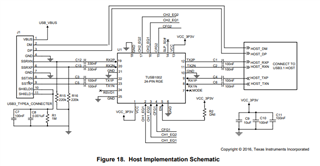
We are trying to layout the traces for the TUSB1002 chip and I am looking at the design recommendations in the TI docs. Which states:
Each pair should be separated at least by 3 times the signal trace width.
However the recommended trace width is 4mils and the impedance 90.
That doesn't really make sense. With our calculations and board calculators we do not get those numbers, not even close for 90 ohm
If you need some additional data for the case: FR-4, Dielectric Constant: 4.05, Copper thickness: 0x035mm, Dielectric Thickness 3.5mils
We tried 4 different, One for the board manufacturer to get their exact data. Then used some online ones to see thier results, and also just going for the spec to manually calculate it. They all come up about the same. Here is an example for an online one: https://www.everythingrf.com/rf-calculators/differential-microstrip-impedance-calculator
https://www.everythingrf.com/rf-calculators/differential-microstrip-impedance-calculator
https://impedance.app.protoexpress.com/
An additional question on that case would be: Different docs states that the Host should be on the AB side and some it should be on the CD side. Can you please clarify that too?