This thread has been locked.

If you have a related question, please click the "Ask a related question" button in the top right corner. The newly created question will be automatically linked to this question.

TIC12400-Q1: Input Voltage at IN0 pin with ADC saturation

Part Number: TIC12400-Q1

Hello,

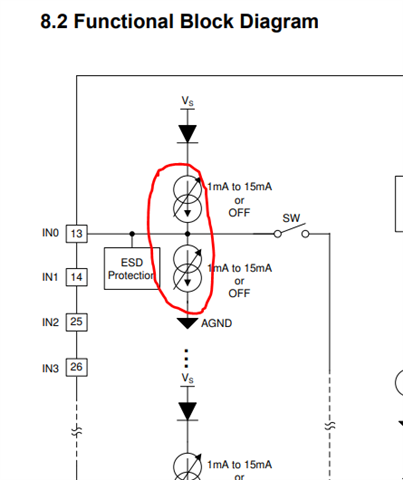
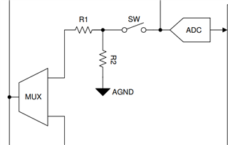
I'm trying to work in ADC mode and I know ADC range is upto 6V. I saw a resistor divider in front of ADC in functional block diagram where i do not know its values. So What is the voltage range i can give to IN0 pin to get the ADC output without saturation? 

  • Hi Akarsh,

    Thanks for reaching out! We might need a bit more clarification to get to the answer here.

    I'm not too sure what resistor divider you're referencing. I looked through the data sheet and didn't see it in our diagrams (but I might have missed it). Though, there is this feature in Section 8.2:

    Is this the part of the block diagram you're referencing? If so, this is not a voltage divider. This is a representation of the current sink/source nodes on each of the INx pins.

    The TIC12400-Q1 provides current sourcing and sinking on each of the INx pins, which create a resulting voltage level on the pin. This is why the device is able to interface with mechanical switches without the need for external components that pull up or pull down on the switch. In other words, this device is not simply a GPIO expander.

    If you're intending to use the ADC for interfacing a resistor-coded switch, I'd recommend looking particularly at Section 8.3.8.2 of the data sheet, which gives a brief definition of the modes of the device.

    Please let me know if you were referencing a different part of the data sheet, or if I can help clarify anything else.

    Best,

    Danny

  • Hello TI team, Thanks for the response.

    Actually I was talking about the resistor dividers in the functional block diagram.

    Now i understood that, if I'm using ADC method, INx pin shall be see a voltage level below 6V to avoid ADC saturation. 

    Now I have other doubt;

    As i mentioned above, Im using ADC with IN2 connected with SW to 24V battery in CSI with 10mA wetting current. Inorder to make the voltage level under 6v , do I need to consider the current sink also in my design ?

    As per the document "Protecting 12-V MSDI Devices in a 24-V System" , i think CSI is not considered. But in my circuit, i believed current sink should be considered. reference is given below. Could you please clarify me?

    Thanks in advance!

    Akarsh V

  • Akarsh,

    Actually I was talking about the resistor dividers in the functional block diagram.

    Now i understood that, if I'm using ADC method, INx pin shall be see a voltage level below 6V to avoid ADC saturation. 

    Ok, thank you for the clarification here! I am glad this part is cleared up. The ADC range is defined based upon the external circuitry, and R1/R2 are not necessarily relevant here.

    As i mentioned above, Im using ADC with IN2 connected with SW to 24V battery in CSI with 10mA wetting current. Inorder to make the voltage level under 6v , do I need to consider the current sink also in my design ?

    For this, yes, an external current source would be relevant. You would need to consider this with the current source being used internally on IN2. Are you just trying to use the TIC12400-Q1 to detect the state of S1?

    Best,

    Danny

  • Hello Danny,

    Thanks for the response.

    Yes I'm trying to monitor the state of S1(this is one of our input) and the monitoring of the Switch is safety critical . so we have to detect the Short detection (to gnd, VBAT, neighboring pins) , Open detection .

    Do you have a suggestion , how to differentiate Short to ground and Open circuit in the above design? 

    Is it possible to turn off the wetting sink current and monitor the INx voltage with ADC?

  • Akarsh,

    Understood. Yes, turning off the wetting current is an option, and then using the input as an analog input would possibly simplify your design. Let me know what you think:

    This setting can be configured using the WC_CFG0 and related registers, which are shown starting on page 80 of the data sheet. By default, the reset value of each of these is set to 0h, which is no wetting current, but you can write as needed here anyway.

    Setting it up without wetting current in ADC mode would be an option as you mentioned.

    Best,

    Danny

  • Hello Danny,

    If we are not using internal wetting current and configuring ADC for our monitoring, 

    1. What will be minimum Vs pin supply voltage for which ADC will work perfectly upto 6V?

    2.Whether the below table is applicable for my design?

    3. In this case, am i able to detect 0V by the internal ADC? in other words, if Im not using current sink , do i need to provide head room voltage of 1.5V at INx pin?

  • Akarsh,

    You'd need to set VS to at least 6.5 V to get the widest range, but even then, the ADC might not be perfectly linear with an input above 5 V. You can see in many of the Typical Characteristics "ADC Code vs. Equivalent Input Resistance" curves that there is an elbow as low as 5 V (based on I*R). Of course, this is a bit dependent upon the current source as well, so turning off the ADC should result in improved performance to linearize this region further.

    In fact, the table you posted is largely why there are bends on the upper ends of these curves. The current sources are not 100% perfect. But here you are not using one.

    You should be good down to 0, as ADC offset error is usually within 1 LSB. But keep in mind the full-scale error of 10 LSB for the ADC as well.

    Best,

    Danny