This thread has been locked.

If you have a related question, please click the "Ask a related question" button in the top right corner. The newly created question will be automatically linked to this question.

SN65DSI83-Q1: Timing variation of LVDS output

Part Number: SN65DSI83-Q1
Other Parts Discussed in Thread: SN65DSI83

Hello team,

My customer use SOC-->SN65DSI83-->DS90UB927-->DS90UB928(display module) in their application.

Display company met flicker issue and  insisted root cause is H-blank has variation at 928 LVDS output.

but 927/928 device use internal PCLK and sync with output so that this doesn't have variation.

So my customer question if SN65DSI83 device can generate Hblanking parameter variation a little.

Could you pls help me answer this to customer??

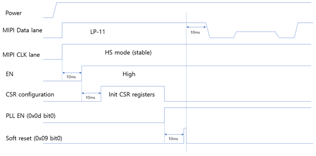
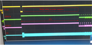
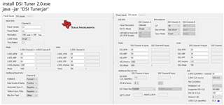
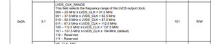
Attached is DSI tuner setting and timing info.

9_2inch_set.pptx

Thank you.

  • Hi,

    Have they tried test pattern, which is internally generated by the DSI83, to see if the flicker issue goes away?

    Please also see this e2e guide on debugging the flicking issue, https://e2e.ti.com/support/interface-group/interface/f/interface-forum/990480/faq-sn65dsi84-how-to-debug-flickering-video-with-sn65dsi83-sn65dsi84-and-sn65dsi85.

    Thanks

    David 

  • Hello David,

    As your guided, I asked customer to try patgen to verify this.

    They will do this. I will update once get test result.

    BTW, Customer is still asking if Hblanking has variation when convert from DSI to LVDS.

    Could you pls help answer this to customer??

    Thank you.

  • Hi,

    There is no need to match horizontal or vertical video CSR configurations to the DSI input values except for the CH*_ACTIVE_LINE_LENGTH (number of active pixel). In other words, as long as the line time is met, the blanking parameters on the LVDS side do not need to exactly match the blanking parameters on the DSI side. However, the active pixels always need to match. So I don't believe the blanking variation comes from the DSI83.

    Thanks

    David

  • Hello David,

    My customer still couldn't resolve this issue.

    This is register configuration by DSI tuner which my customer use for this project and condition is also attached.

    8357.9_2inch_set.pptx

    //=====================================================================
    // Filename   : CSR.txt
    //
    //   (C) Copyright 2013 by Texas Instruments Incorporated.
    //   All rights reserved.
    //
    //=====================================================================
    0x09              0x00
    0x0A              0x03
    0x0B              0x10
    0x0D              0x00
    0x10              0x26
    0x11              0x00
    0x12              0x24
    0x13              0x00
    0x18              0x78
    0x19              0x00
    0x1A              0x03
    0x1B              0x00
    0x20              0x00
    0x21              0x05
    0x22              0x00
    0x23              0x00
    0x24              0x00
    0x25              0x00
    0x26              0x00
    0x27              0x00
    0x28              0x21
    0x29              0x00
    0x2A              0x00
    0x2B              0x00
    0x2C              0x28
    0x2D              0x00
    0x2E              0x00
    0x2F              0x00
    0x30              0x14
    0x31              0x00
    0x32              0x00
    0x33              0x00
    0x34              0x32
    0x35              0x00
    0x36              0x00
    0x37              0x00
    0x38              0x00
    0x39              0x00
    0x3A              0x00
    0x3B              0x00
    0x3C              0x00
    0x3D              0x00
    0x3E              0x00
    
    
    The PLL_EN bit and SOFT_RESET bit are not set as they need to be set per the recommended sequence defined in the datasheet

    Here are some experiment from customer.

    1) Try to disable PLL_EN(0x0d) and re-enable, issue is resolved.

    2) When change OLDI CLK (0x0a) from 0x83 to 0x85, issue is resolved for issue sample. but other normal sample has flicker issue.

    Then My customer is asking onsite support.

    So I need your help what item I need to check.

    1) Check if system meets initialization sequence as datasheet.

    Do you have other items for me to debug this??

    Thank you.

  • Hi,

    I would follow the debugging guide here, https://e2e.ti.com/support/interface-group/interface/f/interface-forum/1101590/sn65dsi83-q1-timing-variation-of-lvds-output

    1) Make sure the initialization sequence follows the table 2 in the datasheet, particularly after power is applied and stable, the DSI CLK lanes MUST be in HS state and the DSI data lanes MUST be driven to LP11 state

    2) Enable test pattern and make sure test pattern is ok. 

    3) Disable test pattern and check the line time on the DSI side

    Thanks

    David

  • Hello David,

    Thanks for your support kindly.

    Can I have quick question??

    1) For init sequence, particularly for condition of HS state and DSI data lane in LP state, if system cannot support this sequence, is there any workaround to cover this?? PLL reset(0x0d bit0)?? or soft reset(0x09 bit0)??

    2) If init sequence is incomplete, error flag always keep high even trying write 0xff to 0xe5 to clear register??

    Thank you.

  • Hi,

    They must follow the initialization sequence, device operating can not be guaranteed without following the sequence. And they need to follow the correct sequence and then see if the error in the status register is still being reported.

    Thanks

    David

  • Hello David,

    Thanks for support.

    My customer ask me to init sequence flow diagram for their easy understanding.

    so I drew it as below.

    Is this correct??

    Thank you.

  • Thank you David, This is really helpful for me.

    I shared this with customer and customer gave their sequence as below.

    They are sure that they meet init sequence and I also agree with them.

    Now, only 1 sample has issue since they have been used this device in this project for 4 years. and 1 time issue happen per 10 times power on trials.

    so I would like guide them to go to quality team for further check.

    Do yo still have another advice for analysis??

    BTW, customer reported 1 weird test experiment is that if they change LVDS CLK range from 001 to 000 in CSR (OLDI clock customer uses=61MHz) , issue doesn't happen. do you have any similar experience??

    Thank you.

  • Hi,

    Have they done these two experiments?

    2) Enable test pattern and make sure test pattern is ok. 

    3) Disable test pattern and check the line time on the DSI side

    They can also do a ABA swap to see if the issue follows the board or the device.

    Thanks

    David

  • Hello David,

    1) Yes, they did patgen test and result is OK. no issue happen.

    2) Asked them to check line time on DSI side.

    3) They will ask approval from OEM(VW) if they can do ABA swap.

    For 1 quick question, LG report their test experiment to VW.

    VW questioned what LVDS CLK range is for??

    I understand this register is to configure OLDI PLL VCO range and this will be adjust according to OLDI clock requirement.

    Am I right??

    Thank you.

  • Hi,

    Both the LVDS_CLK_RANGE and CH_DSI_CLK_RANGE must be set to the frequency range of the LVDS output clock and DSI Channel A input clock respectively for the DSI83-Q1 internal PLL to operate correctly.

    Thanks

    David

  • Hello David,

    I am sorry that customer need more detailed explanation about this.

    I understand this should be PLL VCO band selection according to OLDI clock requirement.

    Am I right?

    Thank you. 

  • Hi,

    I do not have the detailed PLL implementation information for the DSI83-Q1, but most likely the register sets up the correct PLL VCXO range.

    Thanks

    David

  • Hello David,

    Even LG meet power on sequence as datasheet, flicker issue happen with more sample.

    Issue sample #1, failure rate is 1/22 cycle on/off test. (no error flag in register 0xe5)

    issue sample #2, failure rate is 1/51 cycle on/off test. (no error flag in register 0xe5)

    but Issue doesn't happen when change LVDS CLK RANGE value (address 0x0a) from 0x03 to 0x01 for 1000 times cycle test on 2ea issue samples.

    //=====================================================================
    // Filename   : CSR.txt
    //
    //   (C) Copyright 2013 by Texas Instruments Incorporated.
    //   All rights reserved.
    //
    //=====================================================================
    0x09              0x00
    0x0A              0x03
    0x0B              0x10
    0x0D              0x00
    0x10              0x26
    0x11              0x00
    0x12              0x24
    0x13              0x00
    0x18              0x78
    0x19              0x00
    0x1A              0x03
    0x1B              0x00
    0x20              0x00
    0x21              0x05
    0x22              0x00
    0x23              0x00
    0x24              0x00
    0x25              0x00
    0x26              0x00
    0x27              0x00
    0x28              0x21
    0x29              0x00
    0x2A              0x00
    0x2B              0x00
    0x2C              0x28
    0x2D              0x00
    0x2E              0x00
    0x2F              0x00
    0x30              0x14
    0x31              0x00
    0x32              0x00
    0x33              0x00
    0x34              0x32
    0x35              0x00
    0x36              0x00
    0x37              0x00
    0x38              0x00
    0x39              0x00
    0x3A              0x00
    0x3B              0x00
    0x3C              0x00
    0x3D              0x00
    0x3E              0x00
    
    
    The PLL_EN bit and SOFT_RESET bit are not set as they need to be set per the recommended sequence defined in the datasheet

    Do you have any expected root cause?? I think something there is some error when transfer data from DSI to LVDS.

    Now, issue is reported to customer VW and we will need to support this urgently.

    Could you pls support me to resolve this??

    Thank you.

  • Hi,

    This looks to be an issue with the DSI Tuner SW because the SW generates the Bit Field Value to be 001 but the CSR ADDR Value to be 0x03, so there is an issue with the SW when converting from the Bit Field Value to the CSR ADDR Value. 

    If you look at the datasheet, 001 is the correct value for the 61MHz LVDS output clock.

    Thanks

    David

  • Hello David

    This setting is start from bit1 not bit0.

    so I understand register value 0x03 is correct for 61MHz LVDS CLK Range.

    What do u think about it??

    Thanks

  • Hi,

    Correct, I missed the bit 0, so the register value will be 0x03 with DSI_CLK as the clock source. So the DSI Tuner SW is correct and they are not following the recommend register programming value.

    Thanks

    David

  • Hello David,

    Yes. problem is issue happen even LG use correct setting. (0x03). and as their issue verification, Issue is resolved when they use 0x01. 

    That is problem. For now, they have 3pcs issue sample. flicker issue is caused by LVDS output H blanking variation as their verification result by LVDS debug board.

    Have you known any similar issue like customer's verification result??

    Thank you.

  • Harry

    On these three pieces, have they physically measured the LVDS clock output and compare the waveform against a known good unit? 

    I haven't heard anyone reporting this type of issue in the past.

    Thanks

    David 

  • Hello David.

    LVDS CLK output is same between NG chip and Good chip.

    but I cannot analyze LVDS data directly to see if timing is correct.

    That is why LG use LVDS convertor to read timing information via converter register.

    Thank you.

  • Hi, Harry

    What is the exact LVDS CLK frequency you are measuring? Since they are using the DSI CLK as the input clock and LVDS CLK gets derived from the DSI CLK, can you also measure the DSI CLK frequency?

    The LVDS_CLK_RANGE must be set to the frequency range of the LVDS output clock to select the appropriate settings for the internal PLL, so if they changed the LVDS_CLK_RANGE and solve the flickering issue, my expectation is that we will see some difference between a good part and a bad part.

    Besides the clock frequency measurement request, can they also,

    1. Check the line time on the DSI side? 

    2. Do the ABA part swap

    Thanks

    David

  • Hello David,

    for 1) Let me provide line time once get data from customer.

    for 2) Yes, issue follow sample.

    1more information is they use burst mode. is there any configuration is needed for this??

    and I found another similar issue in E2E as below.

    (+) SN65DSI83-Q1: DE period has +/- 1clk - Interface - INTERNAL forum - Interface - INTERNAL - TI E2E support forums

    Do you remember what cause issue??

    Thank you.

  • Hi, Harry

    That issue in the e2e ticket still refers to the fact that the line time on DSI side must match with the line time on the LVDS output. I never received any response after my last message, so I am not sure if the line time is the root cause of their issue or not.

    Thanks

    David