This thread has been locked.

If you have a related question, please click the "Ask a related question" button in the top right corner. The newly created question will be automatically linked to this question.

DP83TG720S-Q1: Link synchronisation not working

Part Number: DP83TG720S-Q1

Hi all,

Currently, we're working on a project with the DP83TG720 chip in our new design. Unfortunately, we're facing some difficulties to have the interface up linux-side.

I explain myself.

We're using the latest kernel driver found on your website for this device, which has been backported for our linux kernel 4.14.

The backporting was successful considering I was able to get a new interface from the userland linux with the phy properly initialised following if it is master or slave.

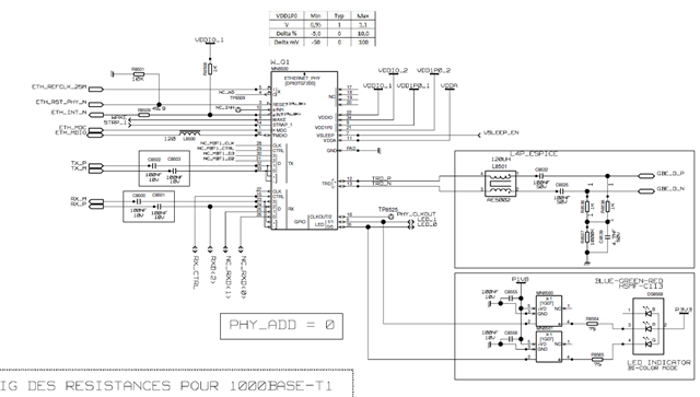
We set the phy as slave in managed mode and we use a 1000BaseT/1000BaseT1 media-converter as master partner.

We know, in managed mode, the PHY is in standby-mode after powering-up and needs to be wake-up by writing 0x0001 to the register 0x018C to start a link synchronisation with a master.

From here, the link synchronisation is not working as expected. Indeed, after starting a link synchronisation, we get our linux interface up but is brought down immediately.

In a repeated way, we're getting a up/down of the interface linux-side. (see below some outputs from debug console).

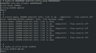
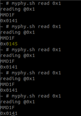
I tried to watch basic registers during a link synchronisation and when polling the BMSR register (0x0001), I get the following values toggling : 0x145/0x141.

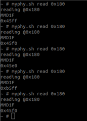
We have the same results with the register C_AND_S_STATUS.

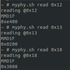
By polling IRQ flags, I noticed the "link_qual_int" bit is set from the register MII_REG_12 (0x0012) saying the link has a bad quality.

Could this flag indicate a hardware problem in our design?

Is there a way to qualify/quantify the link quality?

Thank you very much for your help,

Best Regards,

Arnaud

  • Hi Arnaud,

    Did you use the register setting from the original Linux driver on the website? Is this the link you used for Linux driver: https://www.ti.com/tool/ETHERNET-SW 

    If your register setting is correct, could you send me the schematics of the design?

    --

    Regards,

    Hillman Lin

  • Hi Hillman,

    Thanks for your reply,

    Did you use the register setting from the original Linux driver on the website? Is this the link you used for Linux driver: https://www.ti.com/tool/ETHERNET-SW 

    Yes this is exactly the link I used to get DP83TG720 linux driver.

    I have seen there are 4 register settings and only one is used following the chip id found at probe and if we are master or slave.

    In our case, the chip id is 0x2000a284 matching the following define DP83TG720CS_1_1_PHY_ID.

    As we are slave, the current register setting applied within the driver is : dp83720_cs1_1_slave_init[]

    • I removed the last register (0x18C) in a way to start the link synchronisation by myself from the userland. 

    I checked all registers with a dump from userland and everything seems correct.

    If your register setting is correct, could you send me the schematics of the design?

    Yes, you will find below some schematics of our design (DP83TG720 and power supplies)

    Note we made some changes :

    • R8537 1000K -> 100K

    Thank you for your support,

    Best Regards,

    Arnaud

  • Hi Arnaud,

    • Are you able to read the register from MDIO? if so, Could you provide the information on these could registers: 0001, 0180,0871, and 045D
    • Could you also provide the information on what type of cable you are using? What is your link partner?
    • When I look at your schematics, I have couple of concern:
      • Why are you putting an inductor in series of MDIO pins? Did you have a pull up pins for MDIO?
      • I saw your reset pin has a pull down resistors with 10k ohms. Is there any reason for that?
      • I cannot see your strapping in the schematics, Could you double check on the strapping make sure it is match to your required mode?

    --

    Regards,

    Hillman Lin

  • Hi Hillman,

    Sorry for my late reply but yesterday we finally found out what was the problem on our design.

    In fact, we were using a 25MHz clock generated from a 30,75MHz through a PLL.

    By doing that, we measured, on the generated clock, a jitter around 60ps which is clearly out of range considering the maximum value specified in the datasheet (maximum 1ps).

    So, we swapped our input clock with an internal 100MHz generated elsewhere from our design which is very simple for the PLL to generate the 25MHz-output clock (divided by 4). => the jitter drops to 3ps with the clock swapping.

    After that, we get a solid and steady link up and now we are able to ping the master partner ;-).

    About your questions above

    • Could you also provide the information on what type of cable you are using? What is your link partner?
    • Why are you putting an inductor in series of MDIO pins? Did you have a pull up pins for MDIO?
      • I was told the inductor is here to stabilise the MDIO line cause there are several phy devices sharing the same MDIO bus.
    • I saw your reset pin has a pull down resistors with 10k ohms. Is there any reason for that?
      • Yes, sorry, this is a change I forgot to mention earlier. We swapped the 10K with a 1K.

    Is there any reason to have a maximum jitter of 1ps? (We noticed in a previous datasheet (SNLS604 – SEPTEMBER 2020) we must have a nominal jitter of 3,6ps against maximum 1ps for the REVISED MARCH 2021)

    Thank you very much for your support,

    Best Regards,

    Arnaud

  • Hi Arnaud,

    The reason why we have a maximum jitter of 1ps because we need a clean clock to decrease the signal to noise ratio for testing.

    --

    Regards,

    Hillman Lin

  • Hi Hillman,

    Thank you for your time and support.

    Best Regards,

    Arnaud

  • Hi Arnaud,

    If you have further question. Please reach out to us. Meanwhile we will close this forum.

    --

    Regards,

    Hillman Lin