This thread has been locked.

If you have a related question, please click the "Ask a related question" button in the top right corner. The newly created question will be automatically linked to this question.

TMUXHS4412: Voltage compatibility and capacitor placement

Part Number: TMUXHS4412

Hello Team,

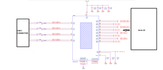
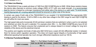
I am using TMUXHS4412 in my design. I have connected the mux to the Arra10 FPGA Serdes (Bank 1G,1H,1I) (Arria 10 Part no:10AX057N2F40E2SG).The supply voltage provided for the MUX is 3.3V.The Bank voltage provided for the Serdes bank is 1.03V

My application is both USB (Host and Device) and DP (Source and sink) data transfer at a speed upto10Gbps.

could you please let me know, Will there be any voltage compatibility issues with the MUX and Arria 10 Serdes. And also will there be a problem with the common-mode voltage of both mux and Arria 10 Serdes.

And also do I need to place capacitors on both sides of the MUX or only the Type C connector side is fine.

I am attaching the block diagram for capacitor placement in my circuit.

Regards,

Tensil Sebastian

  • AC Caps are needed on one side of Mux.

    since DP and USB has different Ac cap value, it's better place Cap on the host side. 

    DP is 100nf for all lanes, USB RX is 300nf an USBTX is 100nf.

    common mode should be fine.

    Regards

    brian

  • Hello Brian,

    Thanks for your valuable comment.

    I have placed capacitors on one side of the MUX.

    If we are using only USB or DP then the cap placement is correct, right. Only the values need to be modified for the DP. Am I correct?

    Regards,

    Tensil Sebastian

  • Hello Brian,

    I have one more query. Hence I don't have any cap on the FPGA side. Will there be any problems regarding the voltage level. Because the Mux is supplied with 3.3V and the FPGA serdes bank is powered with 1.03V.Will this damage my FPGA,hence we don't have any cap between Mux and FPGA.

    Regards,

    Tensil Sebastian

  • MUX supply is 3.3v but IO signal depends on signal spec, if USB or DP, it should be ok.

    Also your comments above is correct.

    Regards

    Brian

  • Hello Brain,

    Thanks for the comments.

    So, finally could you please confirm will my circuit work with the capacitor placed only on the one side of the MUX which is at the connector side.

    Regards,

    Tensil Sebastian

  • Hello Brain,

    I have some more queries,


    In the datasheet, it is recommended that the device is biased from either side of
    the device to a valid value (in the range of 0 - 1.8 V in 3.3 V supply voltage mode).

    1. Does this statement means the MUX has to be biased when in USB/DP transmitter mode and receiver mode on the FPGA Side because another side of the MUX at the connector side is DC blocked by AC Caps?
    2. Will the MUX pass the USB /DP signals in the receiver mode to my FPGA ?? [ At receiver mode FPGA will not have any biasing on the pin]

    Regards,

    Tensil Sebastian

  • Your AC placement should work for either USB or DP only application.

    question 1:yes, Mux will be drived by FPGA common mode voltage.

    2: FPGA receiver should have common mode voltage as well.

    Regards

    Brian