This thread has been locked.
If you have a related question, please click the "Ask a related question" button in the top right corner. The newly created question will be automatically linked to this question.
Hi,
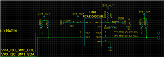
I would like to work with PCA9306 with the same 3.3v on both of his sides (vref1=vref2=3.3V).
I want the device to be like a buffer from my external I2C interface.
i dont have a controller to set the EN pin, can i connect this pin to external PU res?
or should i connect it like in figure 8-6 on datasheet with EN & VREF2 shorted to 200K res to VCC2?
The PCA9306 is not a buffer but a passive switch.
If you want to increase the drive strength, use a buffer like the TCA9800.
but if i use it as a passive switch and i doesnt have how to set the EN pin? how should i connect the EN pin to have the switch open?
If you want to use this device as a switch, you can leave VREF1/2 open, and connect EN directly to 3.3 V or GND.
Consider using an actual switch like the SN74LVC2G66 instead.
if i use PCA9306 as in figure 8-5 on data sheet how i should connect the EN pin? (without gpio from controller)
If you do not have a GPIO, how do you want to control the switch? What is the purpose of the PCA9306 if it is always enabled?
Hi Roei,
If you are connecting VREF2 to a 3.3V supply you have to have a 200K resistor between the power supply and VREF2. This resistor is required to limit the current entering the VREF2 pin.
To go along with what Clemens is saying, what is the "external PU res"?
Best,
Chris
Hi, please see my design attached in the picture below.
can you conform that the buffer will be open and work with the I2C connection?
This circuit will work.
However, the PCA9306 has no effect; it is not a buffer but a passive switch. You can replace it with two wires.
Thanks for the help Clemens!
Roel,
Please let us know if you have any other questions.
Regards,
Eric Hackett