This thread has been locked.

If you have a related question, please click the "Ask a related question" button in the top right corner. The newly created question will be automatically linked to this question.

SN75LVDS83B: SN75LVDS83B issue

Part Number: SN75LVDS83B

Hi team,

Customer has meet an issue on SN75LVDS83B.

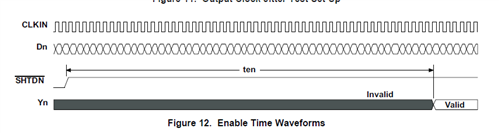
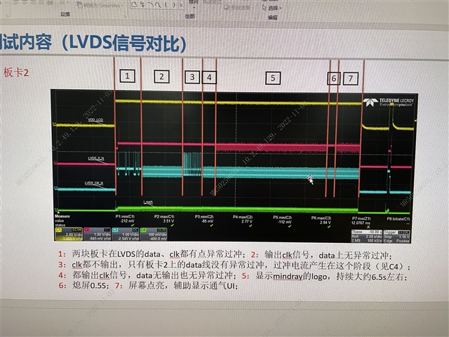
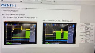
After power up VDD and SHTDN is tied on VDD, CLKIN pin accept a period of CLK from CPU but no valid data. Then customer found some abnormal pulsers output at Y0M. you can refer to attached waveform. The left graph shows LVDS input signal on D0-D7 (green) and output signal on Y0M (yellow). The right graph shows CLKIN(green) and output signal on Y0M (yellow). The abnormal output appears before and after the period of clk without input.

I’m suspecting that when CLKIN has input, the device with send clk signal to 7 channels and at that time, no data to output, which may cause some crosstalk from CLK to output. I’m not sure about that.

Could you pls help to comment on this issue? Thanks!

Thanks!

BR.

Rayna

  • Hi Rayna,

    When SHTDN is toggled high, there is a specific enable time where the data coming from the outputs is not valid. This time Ten is usually 6µs. Is the customer sending a constant clock to the SN75LVDS83B once it is turned on?

    Regards,

    Jack

  • Hi Jack,

    Customer tied VDD and SHDTN together, and customer give clk signal after 1~2s power on. you can refer to below signal waveform. The blue one is clk. In period 1, the clk signal seems affected by noise or something. In period 2 and 5, the clk is normal.

    Rayna

  • Hi Rayna,

    Is the customer using an eval board for the SN75LVDS83B or are they using a custom board? If they are using a custom board, could you send the layout? Let's make sure there isn't crosstalk or coupling.

    How are the signals being measured in the above photos? Do you have a picture of your setup?

    Regards,

    Jack