This thread has been locked.

If you have a related question, please click the "Ask a related question" button in the top right corner. The newly created question will be automatically linked to this question.

SN65HVD1781-Q1: parasitic power drain from the bus?

Part Number: SN65HVD1781-Q1

My design has two channels, each utilizes a bunch of SN65HVD1781-Q1 transceivers and they share a bus on a single PCB. Each channel has common bus, but separate power (but with common ground) and separate HW watchdog.
When I powered up one channel it seemed that everything was working fine, however upon powering up the second channel while first one is active (but no traffic there - transceivers are powered up but idle) power buses (in this case +3V3) do not drop to 0V during the watchdog reset unless both of the watchdogs disable the power at the same time.

I have de soldered the transceivers from one channel and voltages on power rails are now dropping to 0V.
Next I have prepared a simple test board with only said transceiver on it, and connected it to the bus and GND as shown on schematic below:


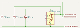
and here are the results (mind that those negative peaks towards 0V is watchdog's doings) :

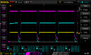
Looks like the transceiver is draining power from the bus to me, am I wrong?
Is this expected to be like that?

  • Hi Jan,

    In your test circuit - why is the "A" voltage being pulled higher than VCC?  Is it possible to show the entire test circuit - as I am a bit confused where the voltages are coming from (output on A/B pins will not be > VCC unless its being pulled up somewhere else. 

    Please let me know as I am having a bit of trouble understanding the issue - as I am having making sense of the graph versus setup you have sent over.

    Best,

    Parker Dodson

  • The A and B pins are connected to A and B lines of the active RS485 bus held in "mark" state until watchdog shuts it off. There is nothing but the oscilloscope probe connected to the Vcc pin - that's why A pin has higher potential than Vcc. The device itself can't get the power from anywhere else than the bus itself, as you noticed and I share your belief on that matter and the test circuit was built to test just that. 
    I wanted to be sure that I'm not wrong about that power thing and to know if this is expected behaviour of this transceiver. 

  • Hi Jan,

    Alright - thanks for the clarification! 

    So in general no - there shouldn't be back powering to the VCC pin from the bus. The driver will  have a diode + transistor between VCC and A or B so current only flows one way. If the pin is essentially floating there may be a voltage that could be read as the probe may be high enough impedance to not pull down the bus - but I am unsure.

    Are you noticing any functional problems besides the VCC showing up with no power (but signal present on bus pins?. Also is it possible to try to make a continuity check with a multi-meter to check if there is a "low" impedance path from A or B to VCC? Can the device signal normally? 

    Please let me know!

    Best,

    Parker Dodson