- Ask a related questionWhat is a related question?A related question is a question created from another question. When the related question is created, it will be automatically linked to the original question.
This thread has been locked.
If you have a related question, please click the "Ask a related question" button in the top right corner. The newly created question will be automatically linked to this question.
I have a modified version of the TCAN demo working with MSP-EXP430FR5994 and TCAN4550 EVM. I can see the CAN packets on the PCAN analyzer.
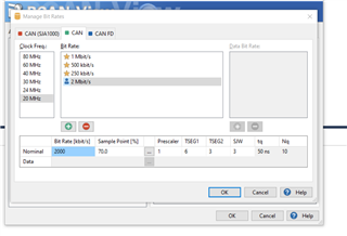
The custom PCB has a TCAN4551 chip and a 20MHz oscillator. I need help setting up the TCAN registers and the PCAN analyzer settings because the same demo project does not generate CAN packets on the PCAN analyzer. The CAN SPI CLK is 2MHz. Does this mean the CAN bit rate is 2kbps? Pasted below are my settings in the PCAN analyzer.
I did try changing the CLK_REF in the device configuration to 0, but nothing changed.
The existing production PCB also uses a 20 MHz crystal to the TCAN chip. Here is how to TCAN driver is setup in this project:
    TCAN4x5x_Device_ClearSPIERR();                              // Clear any SPI ERR flags that might be set as a result of our pin mux changing during MCU startup

    /* Step one attempt to clear all interrupts */
    TCAN4x5x_Device_Interrupt_Enable dev_ie = {
        .word = 0x0UL
    };
    TCAN4x5x_Device_ConfigureInterruptEnable(&dev_ie);          // Disable all non-MCAN related interrupts for simplicity

    TCAN4x5x_Device_Interrupts dev_ir = {
        .word = 0x0UL
    };                                                          // Setup a new MCAN IR object for easy interrupt checking
    TCAN4x5x_Device_ReadInterrupts(&dev_ir);                    // Request that the struct be updated with current DEVICE (not MCAN) interrupt values

    // If the Power On interrupt flag is set
    if (dev_ir.PWRON) {
        TCAN4x5x_Device_ClearInterrupts(&dev_ir);               // Clear it because if it's not cleared within ~4 minutes, it goes to sleep
    }

    /* Configure the CAN bus speeds */
    TCAN4x5x_MCAN_Nominal_Timing_Simple TCANNomTiming = {
        .NominalBitRatePrescaler    = 1,
        .NominalTqBeforeSamplePoint = 32,
        .NominalTqAfterSamplePoint  = 8
    };  // 500k arbitration with a 20 MHz crystal ((20E6 / 2) / (32 + 8) = 500E3)

    TCAN4x5x_MCAN_Data_Timing_Simple TCANDataTiming = {
        .DataBitRatePrescaler = 1,
        .DataTqBeforeSamplePoint = 15,
        .DataTqAfterSamplePoint = 5
    };  // 1 Mbps CAN FD with a 40 MHz crystal (40E6 / (15 + 5) = 2E6)

    /* Configure the MCAN core settings */
    TCAN4x5x_MCAN_CCCR_Config cccrConfig = {
        .FDOE = FDOE_CONFIG,  // Configure CAN FD mode
        .BRSE = BRSE_CONFIG   // Configure CAN BRS
    };

    /* Configure the default CAN packet filtering settings */
    TCAN4x5x_MCAN_Global_Filter_Configuration gfc = {
        .RRFE = 1,                              // Reject remote frames (TCAN4x5x doesn't support this)
        .RRFS = 1,                              // Reject remote frames (TCAN4x5x doesn't support this)
        .ANFE = TCAN4x5x_GFC_REJECT,            // Default behavior if incoming message doesn't match a filter is to reject (29-bit)
        .ANFS = TCAN4x5x_GFC_REJECT,            // Default behavior if incoming message doesn't match a filter is to put if FIFO1 (11-bit)
    };

    /* ************************************************************************
     * In the next configuration block, we will set the MCAN core up to have:
     *   - 2 SID filter element
     *   - 1 XID Filter element (disabled)
     *   - 64 RX FIFO 0 elements (max size)
     *   - RX FIFO 0 supports data payloads up to 64 bytes
     *   - RX FIFO 1 and RX Buffer will not have any elements, but we still set their data payload sizes, even though it's not required
     *   - No TX Event FIFOs
     *   - 2 Transmit buffers supporting up to 64 bytes of data payload
     */

    TCAN4x5x_MRAM_Config MRAMConfiguration = {
        .SIDNumElements = 2,                        // Standard ID number of elements, you MUST have a filter written to MRAM for each element defined
        .XIDNumElements = 1,                        // Extended ID number of elements, you MUST have a filter written to MRAM for each element defined
        .Rx0NumElements = 2,                        // RX0 Number of elements
        .Rx0ElementSize = MRAM_8_Byte_Data,         // RX0 data payload size
        .Rx1NumElements = 64,                       // RX1 number of elements
        .Rx1ElementSize = MRAM_8_Byte_Data,         // RX1 data payload size
        .RxBufNumElements = 0,                      // RX buffer number of elements
        .RxBufElementSize = MRAM_8_Byte_Data,       // RX buffer data payload size
        .TxEventFIFONumElements = 0,                // TX Event FIFO number of elements
        .TxBufferNumElements = 2,                   // TX buffer number of elements
        .TxBufferElementSize = MRAM_8_Byte_Data     // TX buffer data payload size
    };

    /* Configure the MCAN core with the settings above, the changes in this block are write protected registers,      *
     * so it makes the most sense to do them all at once, so we only unlock and lock once                             */

    TCAN4x5x_MCAN_EnableProtectedRegisters();                   // Start by making protected registers accessible
    TCAN4x5x_MCAN_ConfigureCCCRRegister(&cccrConfig);           // Enable FD mode and Bit rate switching
    TCAN4x5x_MCAN_ConfigureGlobalFilter(&gfc);                  // Configure the global filter configuration (Default CAN message behavior)
    TCAN4x5x_MCAN_ConfigureNominalTiming_Simple(&TCANNomTiming);// Setup nominal/arbitration bit timing
    TCAN4x5x_MCAN_ConfigureDataTiming_Simple(&TCANDataTiming);  // Setup CAN FD timing
    TCAN4x5x_MRAM_Clear();                                      // Clear all of MRAM (Writes 0's to all of it)
    TCAN4x5x_MRAM_Configure(&MRAMConfiguration);                // Set up the applicable registers related to MRAM configuration
    TCAN4x5x_MCAN_DisableProtectedRegisters();                  // Disable protected write and take device out of INIT mode

    /* Set the interrupts we want to enable for MCAN */
    TCAN4x5x_MCAN_Interrupt_Enable mcan_ie = {
        mcan_ie.RF0NE = 1,                                       // RX FIFO 0 new message interrupt enable
    };
    TCAN4x5x_MCAN_ConfigureInterruptEnable(&mcan_ie);           // Enable the appropriate registers

    extern const uint16_t SET_BALANCE_VOLTAGE_BASE;
    // Send Balancing Setpoint Frames From Watchdog to FIFO #0
    TCAN4x5x_MCAN_SID_Filter SID_ID = {
        .SFT    = TCAN4x5x_SID_SFT_CLASSIC,
        .SFEC   = TCAN4x5x_SID_SFEC_PRIORITYSTORERX0,
        .SFID1  = SET_BALANCE_VOLTAGE_BASE,                     // SFID1
        .SFID2  = SET_BALANCE_VOLTAGE_BASE                      // SFID2
    };
    TCAN4x5x_MCAN_WriteSIDFilter(0, &SID_ID);                   // Write to the MRAM

    // Send std frames to FIFO #1.  This is dynamically set by
    SID_ID.SFT   = TCAN4x5x_SID_SFT_RANGE;
    SID_ID.SFEC  = TCAN4x5x_SID_SFEC_PRIORITYSTORERX1;
    SID_ID.SFID1 = 0x200;                                       // SFID1
    SID_ID.SFID2 = 0x20F;                                       // SFID2
    TCAN4x5x_MCAN_WriteSIDFilter(1, &SID_ID);                   // Write to the MRAM

    /* Store ID 0x12345678 as a priority message */
    TCAN4x5x_MCAN_XID_Filter XID_ID = {
        .EFT = TCAN4x5x_XID_EFT_RANGENOMASK,                    // Don't filter (id values are Don't cares)
        .EFEC = TCAN4x5x_XID_EFEC_REJECTMATCH,                  // Ignore
        .EFID1 = 0x12345678,                                    // EFID1 (Classic mode filter)
        .EFID2 = 0x1FFFFFFF                                     // EFID2 (Classic mode mask)
    };
    TCAN4x5x_MCAN_WriteXIDFilter(0, &XID_ID);                   // Write to the MRAM

    /* Configure the TCAN4550 Non-CAN-related functions */
    TCAN4x5x_DEV_CONFIG devConfig = {
        .SWE_DIS          = 0,                                      // Keep Sleep Wake Error Enabled (it's a disable bit, not an enable)
        .DEVICE_RESET     = 0,                                      // Not requesting a software reset
        .WD_EN            = 0,                                      // Watchdog disabled
        .nWKRQ_CONFIG     = 0,                                      // Mirror INH function (default)
        .INH_DIS          = 0,                                      // INH enabled (default)
        .GPIO1_GPO_CONFIG = TCAN4x5x_DEV_CONFIG_GPO1_MCAN_INT1,     // MCAN nINT 1 (default)
        .FAIL_SAFE_EN     = 0,                                      // Failsafe disabled (default)
        .GPIO1_CONFIG     = TCAN4x5x_DEV_CONFIG_GPIO1_CONFIG_GPO,   // GPIO set as GPO (Default)
        .WD_ACTION        = TCAN4x5x_DEV_CONFIG_WDT_ACTION_nINT,    // Watchdog set an interrupt (default)
        .WD_BIT_RESET     = 0,                                      // Don't reset the watchdog
        .nWKRQ_VOLTAGE    = 0,                                      // Set nWKRQ to internal voltage rail (default)
        .GPO2_CONFIG      = TCAN4x5x_DEV_CONFIG_GPO2_NO_ACTION,     // GPO2 has no behavior (default)
        .CLK_REF          = 1,                                      // Input crystal is a 40 MHz crystal (default)
        .WAKE_CONFIG      = TCAN4x5x_DEV_CONFIG_WAKE_BOTH_EDGES     // Wake pin can be triggered by either edge (default)
    };
    TCAN4x5x_Device_Configure(&devConfig);                          // Configure the device with the above configuration
    TCAN4x5x_Device_SetMode(TCAN4x5x_DEVICE_MODE_NORMAL);           // Set to normal mode, since configuration is done. This line turns on the transceiver
TCAN4x5x_MCAN_ClearInterruptsAll(); // Resets all MCAN interrupts (does NOT include any SPIERR interrupts)Hello Priya,
The SPI bit rate is independent of the CAN bit rate. The crystal oscillator or single-ended clock applied to the OSC1 and OSC2 pins is used to operate the digital core and CAN Controller.
The 20 MHz clock will be used to create the CAN bit time. The time it takes for a single clock cycle is called a "Minimum Time Quantum" (mtq) because this is the smallest amount of time that can be produced.
A prescaler can be applied to the clock in order to reduce clock frequency used to create the Time Quantum (tq). If the prescaler is set to 1, then 1 tq = 1 mtq. If a prescaler of 2 is used, then 1 tq = 2 mtq.
A CAN bit has several sections that are made up of an integer number of Time Quantum (tq). To achieve a particular data rate, you simply have to configure the correct number of tq for each section. Therefore to achieve a particular bit rate, or bit period, you need to calculate the number of tq needed to create a bit period of a particular length of time.
A 40MHz clock will create twice the mtq a 20MHz clock will create for a given period of time. Therefore a CAN bit time created with a 40MHz clock will have twice as many tq available for the bit as compared to a 20MHz clock.
For example to create a 2Mbps CAN FD bit rate, you simply divide the clock frequency by desired bit rate frequency (note it must result in an integer value).
20MHz / 2MHz = 10 tq
40MHz / 2MHz = 20 tq
The specific location in the bit period that will be used to sample the bit is set by allocating how many tq are before, and how many tq are after this location. Typically the sample point is between 70-80%. It is important for this point to match for all devices, or bit errors may occur.
Now with that said, you just need to make the TCAN4550 settings match your PCAN analyzer settings. Your code looks like you are using a 20MHz clock for your Nominal or Arbitration bit rate calculations and settings, and then using a 40MHz clock for your CAN FD Data bit rate settings. So you will need to change the Data Timing to the following:
TCAN4x5x_MCAN_Data_Timing_Simple TCANDataTiming = {
.DataBitRatePrescaler = 1,
.DataTqBeforeSamplePoint = 7,
.DataTqAfterSamplePoint = 3
}; // 2 Mbps CAN FD with a 20 MHz crystal (20E6 / (7 + 3) = 2E6)
I will note that PCAN Analyzer seems to show 1 too few tq for the bit rate. There are 4 sections to a CAN bit which are the Sync, Prop, Phase1, and Phase2 segments. The Sync seg is always 1 tq. The Prop and Phase1 segments are usually combined into a single grouping as the amount of tq before the sample point (following the sync seg). Phase2 is then just the number of tq after the sample point. It appears the PCAN Analyzer software assumes the sync segment and therefore the total tq show is 1 less than the total and correlates to the amount of tq you have available to allocate.
The TCAN4550's demo code setting for the DataTqBeforeSamplePoint includes the sync seg as part of it's value so that there are only 2 groups to consider in the code and you can verify the number of tq is correct by simply adding the two numbers together (i.e. 7+3=10).
The SJW is the Synchronization Jump Width is usually always set to the same value as Phase2.
I hope that this is a clear explanation on how to determine the settings to create any bit rate.
Also changing the CLK_REF setting will not change the CAN bit timings as I have just explained. It is used to tell the TCAN4550 which clock frequency is applied so that it can use the appropriate internal clock dividers for the internal timers such as the Watchdog and other failsafe timeout timers. If you don't adjust the CLK_REF to match the clock frequency, these timers would still work, but the times would not match the datasheet.
Regards,
Jonathan
Jonathan,
Thank you for your detailed explanation. I will keep the same 1Mbps CAN bit rate as the existing production software with 2MHz SPI clock. Applying your explanation to the CAN settings in the production firmware, the nominal bit rate appears to be 500 kbps and the CAN data rate is 1 Mbps. I want to retain this for the new PCB. Please correct if my understanding is incorrect.
  /* Configure the CAN bus speeds */
    TCAN4x5x_MCAN_Nominal_Timing_Simple TCANNomTiming = {
        .NominalBitRatePrescaler    = 1,
        .NominalTqBeforeSamplePoint = 32,
        .NominalTqAfterSamplePoint  = 8
    };  // 500k arbitration with a 20 MHz crystal ((20E6 / 2) / (32 + 8) = 500E3)

    TCAN4x5x_MCAN_Data_Timing_Simple TCANDataTiming = {
        .DataBitRatePrescaler = 1,
        .DataTqBeforeSamplePoint = 15,
        .DataTqAfterSamplePoint = 5
    };  // 1 Mbps CAN FD with a 40 MHz crystal (40E6 / (15 + 5) = 2E6)
I have set the PCAN analyzer to match the data rates. The PCAN analyzer applies a prescaler of 5 for the nominal bit rate, though I did not select this. I ran the TCAN driver firmware using these settings and he PCAN analyzer is reporting BUSHEAVY status. It didn't make a difference when I changed the nominal bit rate prescaler in the firmware to match the PCAN analyzer, the same status.
 /* Configure the CAN bus speeds */
    TCAN4x5x_MCAN_Nominal_Timing_Simple TCANNomTiming = {
        .NominalBitRatePrescaler    = 5,
        .NominalTqBeforeSamplePoint = 6,
        .NominalTqAfterSamplePoint  = 2
    };  // 500k arbitration with a 20 MHz crystal ((20E6 / 2) / (32 + 8) = 500E3)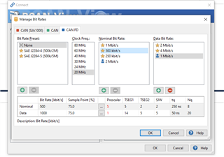
It has been confirmed the power connections to the TCAN4551 are OK, and the incoming SPI signals are also OK. What else is wrong with the CAN driver settings?
Thanks,
Priya
Hello Priya,
Generally the best practice is to try to use as many tq as possible because this improves the accuracy and placement of the sample point within the bit period. Therefore with a 20M clock, a 500k bit would have 40 tq when a pescaler of 1 is used. The sample code shows a 32 - 8 split, which provides an 80% sample point. However the PCAN shows a 75% sample point, and this is not a match. We want to try to match the sample points.
Therefore you can adjust the TCAN4550 allocation to a 30 - 10 split which will provide a 75% sample point to match the PCAN analyzer.
I don't know if you can manually change the prescaler, or the number of tq for the nominal settings in the PCAN analyzer, but if you can use 40tq per bit, this would be better.
You could also use the same settings in the TCAN4550 and apply a prescaler of 5 and allocate 8tq per Nominal bit, but usually more tq per bit is preferred.
Your adjusted bit timings look correct to me in the code. However, I might suggest you update the comment to replace the 40MHz calculation details with your 20MHz calculations. This may be helpful for future reference and avoid confusion.
Regarding the BUSHEAVY status, it is my understanding from what I have read that this can come from either incorrect or incompatible device settings that are preventing the nodes from correctly decoding and acknowledging the messages sent by other nodes, or from too much data or messages on the bus. Incorrect bus termination may also cause this error.
Can you place a scope on the CAN bus signals to verify the bit times from the messages sent by both devices are the same? If so, can you share those plots?
Can you also verify the TCAN status and interrupt registers for any bits that are set and share those values? Registers: 0x000C, 0x0820, and 0x0824. I would also be interested in reviewing the Modes of Operation and Pin Configuration register 0x0800 as well as the MCAN Control Register 0x1018. The Error Counter register 0x1040 and Protocol Status Register 0x1044 will also help on any CAN specific errors.
Regards,
Jonathan
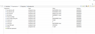
I am waiting for the PCB with jumpers soldered to look at the CAN/SPI lines. In the meantime here is what the IDE reports for the register values. Can you comment to n the SPI and other registers?
I looked at the TCAN4551 datasheet. There is MISO activity in reading the registers. The SPI device ids and revision match the datasheet. SPI status of 0x8 indicates internal access is active which doesn’t seem like a SPI error.
The protocol status register (0x1044) is reporting errors. But the ECR register (0x1040) is not counting errors. I don’t know enough about the other CAN setup registers.

The scope trace shows a 500 kbps bit width. CH3 is CANH and CH2 is CANL. I used the Math function on the scope to display the differential.

Hi Priya,
Actually the PSR register (0x1044) is not showing any errors. The bits that are set are simply indicating that there are "No Changes" in the Last Error Code since the last Read access of this register. The Activity bits state that the bus is Idle and the device is neither transmitting or receiving at the moment.
I noticed the Control register (CCCR with device address 0x1018) shows a value of 0x0. By default the CAN FD operation is disabled and the FD Operation Enable (FDOE bit 8) and Bit Rate Switch Enable (BRSE bit 9) must both be set to '1' in order for a CAN FD message to be transmitted or received. If these bits are set to '0', the CAN controller will throw an error at any CAN FD message. Therefore I suggest setting these bits to '1' and see if the communication errors improve.
Can you also add the Interrupts register (device address 0x0820) to your list of registers that you are monitoring? Register 0x0820 displays the interrupt and status bits for the TCAN4550 device that are not MCAN specific. Register 0x0824 displays the MCAN specific interrupts and this is just a read only copy of the MCAN Interrupt register 0x1050. This read only copy in register 0x0824 is adjacent to the device interrupts in register 0x0820 making it easy to read both sets of interrupts at the same time.
But other device related errors that are reported in register 0x0820 may be occurring that could prevent CAN communication. So it is a good idea to monitor this register as well.
Regards,
Jonathan
Good morning Jonathan,
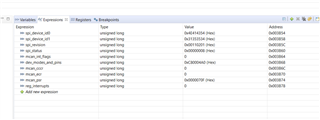
It is good news that the custom board is able to read the CAN SPI id and revision registers correctly. I am capturing this from the IDE at the end of CAN Init routine. However, I don't think my write to the FDOE and BRSE fields is working.
    /* Configure the MCAN core settings */
    TCAN4x5x_MCAN_CCCR_Config cccrConfig = {
        .FDOE = 1,  // Configure CAN FD mode
        .BRSE = 1   // Configure CAN BRS
    };

    bool
TCAN4x5x_MCAN_ConfigureCCCRRegister(TCAN4x5x_MCAN_CCCR_Config *cccrConfig)
{
    uint32_t value, readValue;


    value = cccrConfig->word;
    value &= ~(REG_BITS_MCAN_CCCR_RESERVED_MASK | REG_BITS_MCAN_CCCR_CSA | REG_BITS_MCAN_CCCR_CCE | REG_BITS_MCAN_CCCR_INIT);		// Bitwise AND to get the valid bits (ignore reserved bits and the CCE and INIT)

    // If we made it here, we can update the value so that our protected write stays enabled
    value |= (REG_BITS_MCAN_CCCR_INIT | REG_BITS_MCAN_CCCR_CCE | REG_BITS_MCAN_CCCR_BRSE | REG_BITS_MCAN_CCCR_FDOE);


    AHB_WRITE_32(REG_MCAN_CCCR, value);
#ifdef TCAN4x5x_MCAN_VERIFY_CONFIGURATION_WRITES
    readValue = AHB_READ_32(REG_MCAN_CCCR);

    // Need to do these bitwise ANDs to make this work for clock stop requests and not trigger a false failure when comparing read back value
    if ((readValue & ~(REG_BITS_MCAN_CCCR_RESERVED_MASK | REG_BITS_MCAN_CCCR_CSA | REG_BITS_MCAN_CCCR_CSR | REG_BITS_MCAN_CCCR_CCE | REG_BITS_MCAN_CCCR_INIT))
            != (value & ~(REG_BITS_MCAN_CCCR_RESERVED_MASK | REG_BITS_MCAN_CCCR_CSA | REG_BITS_MCAN_CCCR_CSR | REG_BITS_MCAN_CCCR_CCE | REG_BITS_MCAN_CCCR_INIT)))
    {
        // If our written value and read back value aren't the same, then we return a failure.
        return false;
    }
My current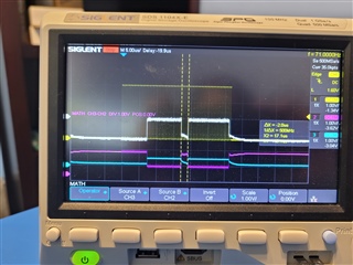 scope trace is also attached
I set the CAN timing registers to match the PCAN analyzer. I continue to get BUSHEAVY status.
It appears the write to the CCCR register does work. Still no changes to the CAN trace on the scope or PCAN analyzer. Awaiting more pointers.
Thanks,
Priya
Hi Priya,
The returned values for your registers do not appear to be correct in your latest post. For example, the Device ID1 (address h0000) should be h4E414354. Your your read back shows that is is h43540002. However, the results from the post before your last one showed the correct values.
I did notice that you appear to have a memory offset error in your code and the register values are shifted by 4 bytes. You can see that the Device ID and Revision register values are split across the different registers with the most significant and least significant values offset from across the register boundary.
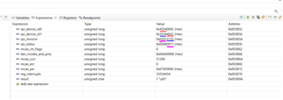
The other register values in your more recent post do not seem correct either and so I can't confirm whether the FD and BRSE bits are getting set in the CCCR register correctly, but I expect they too are not getting set and as a result you are still getting the BUSHEAVY errors.
Can you try to confirm these registers again to ensure the bits are being set according to the values you have set in the code?
Thanks and Regards,
Jonathan
Johnathan,
The last time I captured the screenshot, I may have placed the breakpoint elsewhere. At the end of the CAN init routine, the ide registers are reading their correct values. I am not seeing a SPI status error either.
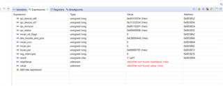
Hi Priya,
Ok this is good news. However, the CCCR register value should not be "0" for CAN FD operation. Bits 8 and 9 (FDOE and BRSE) should both be set to "1" and therefore the register value should something like 0x00000300 after configuration. As long as the BRSE and FDOE bits are set to "0" you can't send CAN FD messages on the bus without getting an error.
If you only sent classical CAN (non-FD) messages, you should not get an error if this is the root cause of the BUSHEAVY error status.
Can you set the FDOE and BRSE bits to "1" and verify they are set by reading them back? Note, these are write protected bits and require both the INIT and CCE bits of this register to both be "1" prior to writing the FDOE and BRSE bits. Otherwise these bits won't get updated. This may require up to 3 writes to get all the bits set to the proper value. Then you will need to do another write to the register to set the INIT (and optionally the CCE) bits back to "0" to resume normal operation.
The example code should handle this, but if these registers are not getting updated, then you should verify there are multiple writes to this register taking place as part of the configuration process.
Regards,
Jonathan
Jonathan,
Is TCAN4x5x_MCAN_EnableProtectedRegisters the right place to set the two bit fields? If it is, it is not happening correctly, the bool returned is false. Please review the function and share if you see errors in this setup. I also tried setting these bits in TCAN4x5x_MCAN_ConfigureCCCRRegister. This function does not have retries. At the end of this function the CCCR does not have the value needed.
bool
TCAN4x5x_MCAN_EnableProtectedRegisters(void)
{
    uint8_t i;
    uint32_t readValue, firstRead;

    firstRead = AHB_READ_32(REG_MCAN_CCCR);

    if ((firstRead & (REG_BITS_MCAN_CCCR_CCE | REG_BITS_MCAN_CCCR_INIT | REG_BITS_MCAN_CCCR_BRSE | REG_BITS_MCAN_CCCR_FDOE)) == (REG_BITS_MCAN_CCCR_CCE | REG_BITS_MCAN_CCCR_INIT | REG_BITS_MCAN_CCCR_BRSE | REG_BITS_MCAN_CCCR_FDOE))
        return true;

    // Unset the CSA and CSR bits since those will be set if we're in standby mode. Writing a 1 to these bits will force a clock stop event and prevent the return to normal mode
    firstRead &= ~(REG_BITS_MCAN_CCCR_CSA | REG_BITS_MCAN_CCCR_CSR | REG_BITS_MCAN_CCCR_CCE | REG_BITS_MCAN_CCCR_INIT | REG_BITS_MCAN_CCCR_BRSE | REG_BITS_MCAN_CCCR_FDOE);
    // Try up to 5 times to set the CCCR register, if not, then fail config, since we need these bits set to configure the device.
    for (i = 10; i > 0; i--)
    {
        readValue = AHB_READ_32(REG_MCAN_CCCR);

        if ((readValue & (REG_BITS_MCAN_CCCR_CCE | REG_BITS_MCAN_CCCR_INIT | REG_BITS_MCAN_CCCR_BRSE | REG_BITS_MCAN_CCCR_FDOE)) == (REG_BITS_MCAN_CCCR_CCE | REG_BITS_MCAN_CCCR_INIT | REG_BITS_MCAN_CCCR_BRSE | REG_BITS_MCAN_CCCR_FDOE))
            return true;
        else if (i == 1)		// Ran out of tries, give up
            return false;
    }
    return true;
}TCAN4x5x_MCAN_ConfigureCCCRRegister(TCAN4x5x_MCAN_CCCR_Config *cccrConfig)
{
uint32_t value, readValue;
value = cccrConfig->word;
value &= ~(REG_BITS_MCAN_CCCR_RESERVED_MASK | REG_BITS_MCAN_CCCR_CSA | REG_BITS_MCAN_CCCR_CCE | REG_BITS_MCAN_CCCR_INIT ); // Bitwise AND to get the valid bits (ignore reserved bits and the CCE and INIT)
// If we made it here, we can update the value so that our protected write stays enabled
value |= (REG_BITS_MCAN_CCCR_INIT | REG_BITS_MCAN_CCCR_CCE | REG_BITS_MCAN_CCCR_BRSE | REG_BITS_MCAN_CCCR_FDOE);
AHB_WRITE_32(REG_MCAN_CCCR, value);
#ifdef TCAN4x5x_MCAN_VERIFY_CONFIGURATION_WRITES
readValue = AHB_READ_32(REG_MCAN_CCCR);
// Need to do these bitwise ANDs to make this work for clock stop requests and not trigger a false failure when comparing read back value
if ((readValue & ~(REG_BITS_MCAN_CCCR_RESERVED_MASK | REG_BITS_MCAN_CCCR_CSA | REG_BITS_MCAN_CCCR_CSR | REG_BITS_MCAN_CCCR_CCE | REG_BITS_MCAN_CCCR_INIT | REG_BITS_MCAN_CCCR_BRSE | REG_BITS_MCAN_CCCR_FDOE))
!= (value & ~(REG_BITS_MCAN_CCCR_RESERVED_MASK | REG_BITS_MCAN_CCCR_CSA | REG_BITS_MCAN_CCCR_CSR | REG_BITS_MCAN_CCCR_CCE | REG_BITS_MCAN_CCCR_INIT | REG_BITS_MCAN_CCCR_BRSE | REG_BITS_MCAN_CCCR_FDOE)))
{
// If our written value and read back value aren't the same, then we return a failure.
return false;
}
// Check to see if the CSR bits are not as expected, since this can be set by the hardware.
if ((readValue & REG_BITS_MCAN_CCCR_CSR) != cccrConfig->CSR)
{
// Then there's a difference in the CSR bits, which may not be a failure.
if (TCAN4x5x_Device_ReadMode() == TCAN4x5x_DEVICE_MODE_STANDBY)
{
// CSR bit is set due to being in standby mode. Not a failure.
return true;
} else {
// It's not matching for some other reason, we've got a real failure.
return false;
}
}
#endif
return true;At the end of the TCAN4x5x_MCAN_ConfigureCCCRRegister the value read does not have the BRSE and FDOE set. Why is this?

Hi Priya,
The TCAN4x5x_MCAN_ConfigureCCCRRegister function will write the value of the "cccrConfig" data struct to the register. This is similar to how the demo code sets the other register bits.
Therefore in the main.c file you should find an "Init_CAN()" function that has all the device struct bit assignments. This is also where the bit timing values are set.
In my version of the demo code, the following lines of code are found immediately following the bit timing settings.
	/* Configure the MCAN core settings */
	TCAN4x5x_MCAN_CCCR_Config cccrConfig = {0};					// Remember to initialize to 0, or you'll get random garbage!
	cccrConfig.FDOE = 1;										// CAN FD mode enable
	cccrConfig.BRSE = 1;										// CAN FD Bit rate switch enable
Then later on in this Init_CAN() function after all the other register bits have been set in the various data structs, you should find a few lines of code that actually write the registers with these bit settings.
	/* Configure the MCAN core with the settings above, the changes in this block are write protected registers,      *
	 * so it makes the most sense to do them all at once, so we only unlock and lock once                             */

	TCAN4x5x_MCAN_EnableProtectedRegisters();					// Start by making protected registers accessible
	TCAN4x5x_MCAN_ConfigureCCCRRegister(&cccrConfig);			// Enable FD mode and Bit rate switching
	TCAN4x5x_MCAN_ConfigureGlobalFilter(&gfc);                  // Configure the global filter configuration (Default CAN message behavior)
	TCAN4x5x_MCAN_ConfigureNominalTiming_Simple(&TCANNomTiming);// Setup nominal/arbitration bit timing
	TCAN4x5x_MCAN_ConfigureDataTiming_Simple(&TCANDataTiming);	// Setup CAN FD timing
	TCAN4x5x_MRAM_Clear();										// Clear all of MRAM (Writes 0's to all of it)
	TCAN4x5x_MRAM_Configure(&MRAMConfiguration);				// Set up the applicable registers related to MRAM configuration
	TCAN4x5x_MCAN_DisableProtectedRegisters();					// Disable protected write and take device out of INIT mode
First, the code enables the protected registers which sets the INIT and CCE bits to "1" through the TCAN4x5x_MCAN_EnableProtectedRegisters() function. This allows the other write protected bits, such as the FDOE and BRSE bits, to be set.
The next function call is TCAN4x5x_MCAN_ConfigureCCCRRegister(&cccrConfig) which will set the FDOE and BRSE bits if they have been set to "1" in the previous lines of code.
After all of the registers that contain write protected bits, the TCAN4x5x_MCAN_DisableProtectedRegisters() function is called to set the INIT and CCE bits back to '0'.
Can you verify you have the lines of code to set the FDOE and BRSE bits in the cccrConfig data struct and that they are setting the bits to '1'?
Regards,
Jonathan
Jonathan,
I was just able to re-use the can_init routine from the TCAN demo today. I removed all the edits I made previously to the TCAN4x5x_MCAN_EnableProtectedRegisters and TCAN4x5x_MCAN_ConfigureCCCRRegister routines. At the end of can_init, the ccr register value looks better. The scope trace I also captured today is not showing TTL amplitude for MOSI and MISO, only for SPI_CLK and CS. Nothing else has changed, still getting BUSHEAVY status. I will continue this tomorrow.
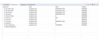
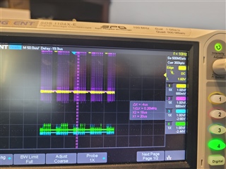
void initCAN (void)
{
uint32_t spi_device_id0, spi_device_id1, spi_revision, spi_status, reg_dev_ir, mcan_int_flags, dev_modes_pins, mcan_cccr, mcan_ecr, mcan_psr;
    TCAN4x5x_Device_ClearSPIERR();                              // Clear any SPI ERR flags that might be set as a result of our pin mux changing during MCU startup

     /* Step one attempt to clear all interrupts */
     TCAN4x5x_Device_Interrupt_Enable dev_ie = {0};              // Initialize to 0 to all bits are set to 0.
     TCAN4x5x_Device_ConfigureInterruptEnable(&dev_ie);          // Disable all non-MCAN related interrupts for simplicity

     TCAN4x5x_Device_Interrupts dev_ir = {0};                    // Setup a new MCAN IR object for easy interrupt checking
     TCAN4x5x_Device_ReadInterrupts(&dev_ir);                    // Request that the struct be updated with current DEVICE (not MCAN) interrupt values

     if (dev_ir.PWRON)                                           // If the Power On interrupt flag is set
         TCAN4x5x_Device_ClearInterrupts(&dev_ir);               // Clear it because if it's not cleared within ~4 minutes, it goes to sleep

     /* Configure the CAN bus speeds */
     TCAN4x5x_MCAN_Nominal_Timing_Simple TCANNomTiming = {0};    // 500k arbitration with a 40 MHz crystal ((40E6 / 2) / (32 + 8) = 500E3)
     TCANNomTiming.NominalBitRatePrescaler = 1;
     TCANNomTiming.NominalTqBeforeSamplePoint = 32;
     TCANNomTiming.NominalTqAfterSamplePoint = 8;

     TCAN4x5x_MCAN_Data_Timing_Simple TCANDataTiming = {0};      // 2 Mbps CAN FD with a 40 MHz crystal (40E6 / (15 + 5) = 2E6)
     TCANDataTiming.DataBitRatePrescaler = 1;
     TCANDataTiming.DataTqBeforeSamplePoint = 15;
     TCANDataTiming.DataTqAfterSamplePoint = 5;

     /* Configure the MCAN core settings */
     TCAN4x5x_MCAN_CCCR_Config cccrConfig = {0};                 // Remember to initialize to 0, or you'll get random garbage!
     cccrConfig.FDOE = 1;                                        // CAN FD mode enable
     cccrConfig.BRSE = 1;                                        // CAN FD Bit rate switch enable

     /* Configure the default CAN packet filtering settings */
     TCAN4x5x_MCAN_Global_Filter_Configuration gfc = {0};
     gfc.RRFE = 1;                                               // Reject remote frames (TCAN4x5x doesn't support this)
     gfc.RRFS = 1;                                               // Reject remote frames (TCAN4x5x doesn't support this)
     gfc.ANFE = TCAN4x5x_GFC_ACCEPT_INTO_RXFIFO0;                // Default behavior if incoming message doesn't match a filter is to accept into RXFIO0 for extended ID messages (29 bit IDs)
     gfc.ANFS = TCAN4x5x_GFC_ACCEPT_INTO_RXFIFO0;                // Default behavior if incoming message doesn't match a filter is to accept into RXFIO0 for standard ID messages (11 bit IDs)

     /* ************************************************************************
      * In the next configuration block, we will set the MCAN core up to have:
      *   - 1 SID filter element
      *   - 1 XID Filter element
      *   - 5 RX FIFO 0 elements
      *   - RX FIFO 0 supports data payloads up to 64 bytes
      *   - RX FIFO 1 and RX Buffer will not have any elements, but we still set their data payload sizes, even though it's not required
      *   - No TX Event FIFOs
      *   - 2 Transmit buffers supporting up to 64 bytes of data payload
      */
     TCAN4x5x_MRAM_Config MRAMConfiguration = {0};
     MRAMConfiguration.SIDNumElements = 1;                       // Standard ID number of elements, you MUST have a filter written to MRAM for each element defined
     MRAMConfiguration.XIDNumElements = 1;                       // Extended ID number of elements, you MUST have a filter written to MRAM for each element defined
     MRAMConfiguration.Rx0NumElements = 5;                       // RX0 Number of elements
     MRAMConfiguration.Rx0ElementSize = MRAM_64_Byte_Data;       // RX0 data payload size
     MRAMConfiguration.Rx1NumElements = 0;                       // RX1 number of elements
     MRAMConfiguration.Rx1ElementSize = MRAM_64_Byte_Data;       // RX1 data payload size
     MRAMConfiguration.RxBufNumElements = 0;                     // RX buffer number of elements
     MRAMConfiguration.RxBufElementSize = MRAM_64_Byte_Data;     // RX buffer data payload size
     MRAMConfiguration.TxEventFIFONumElements = 0;               // TX Event FIFO number of elements
     MRAMConfiguration.TxBufferNumElements = 2;                  // TX buffer number of elements
     MRAMConfiguration.TxBufferElementSize = MRAM_64_Byte_Data;  // TX buffer data payload size


     /* Configure the MCAN core with the settings above, the changes in this block are write protected registers,      *
      * so it makes the most sense to do them all at once, so we only unlock and lock once                             */

     TCAN4x5x_MCAN_EnableProtectedRegisters();                   // Start by making protected registers accessible
     TCAN4x5x_MCAN_ConfigureCCCRRegister(&cccrConfig);           // Enable FD mode and Bit rate switching
     TCAN4x5x_MCAN_ConfigureGlobalFilter(&gfc);                  // Configure the global filter configuration (Default CAN message behavior)
     TCAN4x5x_MCAN_ConfigureNominalTiming_Simple(&TCANNomTiming);// Setup nominal/arbitration bit timing
     TCAN4x5x_MCAN_ConfigureDataTiming_Simple(&TCANDataTiming);  // Setup CAN FD timing
     TCAN4x5x_MRAM_Clear();                                      // Clear all of MRAM (Writes 0's to all of it)
     TCAN4x5x_MRAM_Configure(&MRAMConfiguration);                // Set up the applicable registers related to MRAM configuration
     TCAN4x5x_MCAN_DisableProtectedRegisters();                  // Disable protected write and take device out of INIT mode


     /* Set the interrupts we want to enable for MCAN */
     TCAN4x5x_MCAN_Interrupt_Enable mcan_ie = {0};               // Remember to initialize to 0, or you'll get random garbage!
     mcan_ie.RF0NE = 1;                                          // RX FIFO 0 new message interrupt enable

     TCAN4x5x_MCAN_ConfigureInterruptEnable(&mcan_ie);           // Enable the appropriate registers


     /* Setup filters, this filter will mark any message with ID 0x055 as a priority message */
     TCAN4x5x_MCAN_SID_Filter SID_ID = {0};
     SID_ID.SFT = TCAN4x5x_SID_SFT_CLASSIC;                      // SFT: Standard filter type. Configured as a classic filter
     SID_ID.SFEC = TCAN4x5x_SID_SFEC_PRIORITYSTORERX0;           // Standard filter element configuration, store it in RX fifo 0 as a priority message
     SID_ID.SFID1 = 0x055;                                       // SFID1 (Classic mode Filter)
     SID_ID.SFID2 = 0x7FF;                                       // SFID2 (Classic mode Mask)
     TCAN4x5x_MCAN_WriteSIDFilter(0, &SID_ID);                   // Write to the MRAM


     /* Store ID 0x12345678 as a priority message */
     TCAN4x5x_MCAN_XID_Filter XID_ID = {0};
     XID_ID.EFT = TCAN4x5x_XID_EFT_CLASSIC;                      // EFT
     XID_ID.EFEC = TCAN4x5x_XID_EFEC_PRIORITYSTORERX0;           // EFEC
     XID_ID.EFID1 = 0x12345678;                                  // EFID1 (Classic mode filter)
     XID_ID.EFID2 = 0x1FFFFFFF;                                  // EFID2 (Classic mode mask)
     TCAN4x5x_MCAN_WriteXIDFilter(0, &XID_ID);                   // Write to the MRAM

     /* Configure the TCAN4550 Non-CAN-related functions */
     TCAN4x5x_DEV_CONFIG devConfig = {0};                        // Remember to initialize to 0, or you'll get random garbage!
     devConfig.SWE_DIS = 0;                                      // Keep Sleep Wake Error Enabled (it's a disable bit, not an enable)
     devConfig.DEVICE_RESET = 0;                                 // Not requesting a software reset
     devConfig.WD_EN = 0;                                        // Watchdog disabled
     devConfig.nWKRQ_CONFIG = 0;                                 // Mirror INH function (default)
     devConfig.INH_DIS = 0;                                      // INH enabled (default)
     devConfig.GPIO1_GPO_CONFIG = TCAN4x5x_DEV_CONFIG_GPO1_MCAN_INT1;    // MCAN nINT 1 (default)
     devConfig.FAIL_SAFE_EN = 0;                                 // Failsafe disabled (default)
     devConfig.GPIO1_CONFIG = TCAN4x5x_DEV_CONFIG_GPIO1_CONFIG_GPO;      // GPIO set as GPO (Default)
     devConfig.WD_ACTION = TCAN4x5x_DEV_CONFIG_WDT_ACTION_nINT;  // Watchdog set an interrupt (default)
     devConfig.WD_BIT_RESET = 0;                                 // Don't reset the watchdog
     devConfig.nWKRQ_VOLTAGE = 0;                                // Set nWKRQ to internal voltage rail (default)
     devConfig.GPO2_CONFIG = TCAN4x5x_DEV_CONFIG_GPO2_NO_ACTION; // GPO2 has no behavior (default)
     devConfig.CLK_REF = 1;                                      // Input crystal is a 40 MHz crystal (default)
     devConfig.WAKE_CONFIG = TCAN4x5x_DEV_CONFIG_WAKE_BOTH_EDGES;// Wake pin can be triggered by either edge (default)
     TCAN4x5x_Device_Configure(&devConfig);                      // Configure the device with the above configuration

     TCAN4x5x_Device_SetMode(TCAN4x5x_DEVICE_MODE_NORMAL);       // Set to normal mode, since configuration is done. This line turns on the transceiver

     TCAN4x5x_MCAN_ClearInterruptsAll();                         // Resets all MCAN interrupts (does NOT include any SPIERR interrupts)


     spi_device_id0 = AHB_READ_32(REG_SPI_DEVICE_ID0);
     spi_device_id1 = AHB_READ_32(REG_SPI_DEVICE_ID1);
     spi_revision = AHB_READ_32(REG_SPI_REVISION);
     spi_status = AHB_READ_32(REG_SPI_STATUS);
     reg_dev_ir = AHB_READ_32(REG_DEV_IR);
     mcan_int_flags = AHB_READ_32(REG_MCAN_INT_FLAGS);
     dev_modes_pins = AHB_READ_32(REG_DEV_MODES_AND_PINS);
     mcan_cccr = AHB_READ_32(REG_MCAN_CCCR);
     mcan_ecr = AHB_READ_32(REG_MCAN_ECR);
     mcan_psr = AHB_READ_32(REG_MCAN_PSR);


}
Hi Priya,
It looks like we are making progress and it's good to see that the CCCR register is not getting set correctly. The MOSI/MISO signal levels is an interesting observation. However since you are able to write/read the registers, hopefully this is test setup issue and is not real.
I'm not an expert on the PCAN analyzer tool created by Peak-System so I don't exactly know all of reasons the BUSHEAVY indicator will occur. However, looking at Peak-System support forum, I saw a couple threads that mentioned the BUSHEAVY status.
This first thread has a post that says "a Busheavy can occur when you want to send a CAN-message and no other CAN-node is able to send a acknowlegde frame (wrong baudrate, CAN-bus not connected, no CAN-termination, a CAN-bus system with only one CAN-node etc.)" - (https://forum.peak-system.com/viewtopic.php?t=35 )
Another thread said that the BUSHEAVY indicator occurs with the PCAN node has an error counter greater than 127 and that you can clear this by resetting the node by re-initializing it. - (https://forum.peak-system.com/viewtopic.php?f=120&t=39 )
However, I might make a suggestion to help narrow down whether this is a TCAN4550 or a PCAN configuration issue. Right now we just know that the two devices do not appear to be configured the same way. Since I believe you also have a second TCAN4550 board or setup using a TCAN4550 EVM, and that you try to connect two TCAN4550 devices together with the same settings and see if you can send and receive CAN messages.
This would at least help validate the TCAN4550 settings and the custom board's hardware. Since I know the different interrupt and error flags in the TCAN4550 MCAN controller, I could better help with both the transmit and receive settings on the two boards which we know are compatible because they are both TCAN4550. Would a test like that be possible?
Also, make sure that the CAN bus is properly terminated with a 120 ohm resistor at both ends, or with a single 60 ohm resistor on one of the boards if the wires between the boards are short. Improper bus termination can cause CAN errors which could add up and cause the communication errors.
Regards,
Jonathan
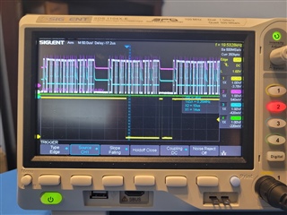
I am seeing the correct CANH-CANL voltage levels (white) this morning on the custom PCB. Two scope probes were set at 10x yesterday. While this is a relief, the PCAN analyzer maintains a BUSHEAVY status. I changed the initCAN routine to use the same tq settings as the PCAN and this doesn't make a difference.
The custom PCB does have one 120 Ohm resistor connected to the CANH line.
Hi Priya,
It's good to knot the signal levels are correct. However, I'm not sure what to make of the large "peaking" on the Dominant to recessive edges because this is larger than I typically see. Is there also a 120 ohm termination on the PCAN analyzer?
How is the bus communication working, as in which board is transmitting, and which one is receiving? Or are they both trying to both transmit and receive at the same time? Despite the BUSHEAVY status, is the RX FIFO receiving new messages, or are the Error Counters logging errors?
Is this setup to continually send messages, or is it trying to send a single message but we are seeing multiple messages because it is not getting acknowledge?
Can you try to only have one board send a message at a time to see if it is received in the RX FIFO or changes the error counters in any way? For example send a message from the TCAN4550 to the PCAN analyzer and check to see if it was received. The TCAN4550 has a DAR bit to Disable Automatic Retransmission that can be set in the CCCR register. This will cause the TCAN4550 to only make a single attempt at sending a message regardless of whether it was acknowledged. This can be useful for testing and debug.
Then can you try to reverse the direction and send a message from the PCAN to the TCAN4550 and see if it was acknowledged and received?
I think we need to try to break down the communication path and isolate whether this is an issue with the TX or RX path between the two nodes so we know which settings need adjustment.
Also, if you have two TCAN4550 boards, can they be tested together without a PCAN analyzer? I don't know if this is possible for your setup or would be too difficult. But it might also help provide some insight on incorrect settings.
Can you also share what the CAN message ID and Data payload is supposed to be so that I can look at the CAN waveforms to see if the bits are matching correctly?
Regards,
Jonathan
The MSP430 is the only processor transmitting messages through CAN. No receive messages from the CAN controller. However, the mcan_ecr is reading 0x80 and mcan_ccr 0x300. I looked closer at the CAN message bitwidth. The thinnest pulse is measuring 500kbps. So maybe there still is a problem with the CAN FD?
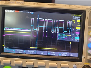
Hi Priya,
The message header is always going to be at the Nominal bit rate, which must be less than 1Mbps, and is 500kbps in your configuration if our timing settings are correct. If that is what you are measuring, then this is validates our timing settings.
If the node wins arbitration, the data rate will increase to the FD bit rate if the message is configured to be a FD message with Bit Rate Switching. Enabling the FDOE and BRSE bits in the CCCR register simply enables the TCAN4550 to be capable of transmitting and receiving an FD message with a faster data bit rate. But this does not guarantee the message will be sent as FD. There are two bits that are in the message header that instruct the controller to send the message as either a classical or FD message, and if it is an FD message whether to switch to a faster bit rate or continue using the Nominal Bit Rate.
If there is a bit rate switch, it will occur at the sample point of the BRS bit in the message header. Here is a table view of a complete CAN FD message where each Row is a single 32-bit word in the message. The top two words T0 and T1 are the message header. The rest of the words T2-Tn are the message's data payload.
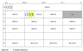
This figure and additional information the MCAN CAN FD controller can be found in the MCAN User's Manual developed by Bosch.
https://www.bosch-semiconductors.com/media/ip_modules/pdf_2/m_can/mcan_users_manual_v330.pdf
Can you tell me the specifics of the message you are sending, or verify that the FD and BRS properly? Also, can you match up the bits in the message header with the CAN waveforms? For example, can you verify the Message ID and other bit values are correct? If they don't match, perhaps there is an issue with the Message RAM (MRAM) allocation and the bytes in the TX Buffer are incorrect.
If however, the message looks to be correctly transmitting from the TCAN4550, then there may be some setting in the PCAN analyzer that is preventing it from acknowledging the messages.
Another thing to look for is to see if the full data payload of the message is getting transmitted on the CAN bus. I don't see an error flag signal on the bus, but CAN errors are thrown immediately when detected, so if the CAN message is shorter than expected, the location of the last bit in the message is a possible clue to the cause.
Also I just noticed in this more zoomed in scope image that the CANH and CANL waveforms don't look quite right to me. Which color trace is CANH, and CANL? One of them should be an inverted copy of the other and the recessive voltage between the dominant bits should be approximately 2.5V. Both the blue and magenta waveforms look to have the same shape and polarity, but with one larger than the other. I also don't see the 2.5V recessive level. If the waveforms are incorrect, then perhaps our settings are OK, and we instead have a hardware issue and incorrect CAN waveforms.
Regards,
Jonathan
Jonathan,
I needed to troubleshoot my setup and hence the delay in my response. Attached are the CAN waveforms on the scope. Pink is CANH and yellow CANL. They don't have the amplitude you describe. I also realized the logic analyzer can decode CAN. I triggered on the falling edge of CANH, at bitrate 1Mbps, 75% sample point. These match the TCANDataTiming from the firmware, let me know if the input to the LA is correct. The data fields don't look like the measurements being transmitted. It will be really good to confirm if the firmware CAN settings are correct. In the header transmitted from the firmware, I set the .FDF and .BRS fields to 1.
TCAN4x5x_MCAN_TX_Header header = {
.DLC = 8,
.id = hdr,
.FDF = HEADER_FDF_CONFIG,
.BRS = HEADER_BRS_CONFIG,
.EFC = 0,
.MM = 0,
.RTR = 0,
.XTD = 0,
.ESI = 0
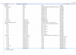
Here is how the firmware is packaging CAN data, which looks correct:
Hi Priya,
Thanks for the additional detailed information. I didn't have time to finish reviewing all of it and provide a response today, so I will follow up with you on this tomorrow.
Regards,
Jonathan
Hi Priya,
The CAN waveforms don't look correct in all regards. The voltage levels do not match CAN physical layer specs, and the bit sequence is not correct from my understanding of your message configuration.
I have tried to duplicate your message and captured the waveforms with a test setup consisting of 2 TCAN4550 devices connected together on a simple bus using the BOOSTXL-CANFD-LIN BoosterPacks attached to MSP-EXP430FR6989 LaunchPads. The 120 ohm termination resistance on both boards is enabled with jumpers to create the 60 ohm bus impedance.
The C1 probe (yellow) is the CANH signal which swings between 2.5V (recessive) and 3.5V (dominant) with respect to GND.
The C2 probe (blue) is the CANL signal which swings between 2.5V (recessive) and 1.65V (dominant) with respect to GND.
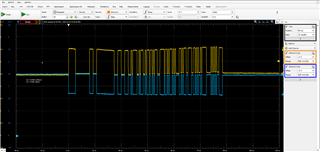
With exception of the Error State Indicator (ESI) bit showing a different value on my board than yours, the message header bits seem to match until a bit into the data payload field. Then the two waveforms start to deviate.
However, what concerns me the most is your CANL waveform. It should be inverted from the CANH waveform and share a common recessive level of approximately 2.5V. Your CANL waveform has the same shape and polarity as the CANH waveform and it has incorrect voltage levels. There is also a lot of ringing noise on the edge transitions that is not seen on the CANH edges. Since this is a differential bus, there should not be such a difference in the noise or amplitude.
It is common to see some difference in amplitude between the CANH and CANL waveforms, but they are intended to be fairly symmetrical.
I noticed in your previous scope plots that the CANH/L waveform levels didn't look correct either. CANH seemed to be almost 3V in amplitude, and CANL was still only 1V and again with the same polarity as CANH. There doesn't seem to be a recessive voltage for either of these signals and they appear to almost go to GND during the recessive bits. Where is the GND reference of your probe during the measurements? Is it connected to GND on the board?
Can you share the schematic for the TCAN4550 circuits and the components on the CANH/L pins for my review?
Regards,
Jonathan
Hi Priya,
Thank you, I have been reviewing the schematic you sent. I now believe I understand the CAN signal levels in your waveforms.
The 10k pulldown resistors on the CANH and CANL are not common and can cause common mode issues with the recessive state voltage levels. The transceiver will drive the CANH to approximately 3.5V and drive CANL to approximately 1.65V during the Dominant bits, and then become high impedance during the Recessive bits allowing the bits to become pulled to a weakly biased 2.5V Recessive Voltage level. Pulldown resistors to GND on CANH and CANL will pull the line voltage down towards GND instead of 2.5V during the Recessive bits and this is why the signals appear the way they do.
The CAN transceiver is a differential receiver looking at the voltage difference between the CANH and CANL so it may be possible to still receive the data with the pulldown resistors on the bus, but this is problematic for several other issues. For example you would probably not be able to pass any RF emissions test standards with these pulldown resistors.
Therefore, I recommend removing the 10k pulldown resistors R208 and R209. Is there a particular reason why they are in the schematic?
I also did not see a 120 ohm termination resistance between CANH and CANL in the schematics. The CAN bus should have two 120 ohm termination resistors for a total parallel resistance of 60 ohms. These termination resistors should be placed at the two ends of the bus. When you are doing a test with only two nodes such as one PCAN Analyzer and one TCAN4550 board, a 120 ohm termination resistor should be on each node. If there are more than 2 nodes, the middle nodes on the bus do not need the termination.
In a previous message you mentioned the custom PCB had a 120 ohm resistor on the CANH line, but I didn't see it. Is this 120 ohm resistor placed between the CANH and CANL pins during our debug efforts? Or are you applying external termination on the wiring harness itself? Please make sure the CAN bus termination is correct because incorrect termination can also result in errors.
You also mentioned that the MSP430 is the only processor transmitting messages through CAN. No receive messages from the CAN controller. Have you tried to send messages from the PCAN to the TCAN4550 to see if it can receive messages? I would like to know if there are errors on both directions of communication between the two boards, or if the errors are only in one direction.
Can you remove the pulldown resistors, verify there is a total impedance of 60 ohms between CANH and CANL, and retest the communication so see if there are any improvements?
Regards,
Jonathan
H Ptiya,
Thanks for pointing it out. I don't know how I overlooked it it.
Regards,
Jonathan
Jonathan,
The production PCB has the same two resistors you mentioned. Scope traces of the CAN waveforms in this PCB will be gathered. I also noticed that the production PCB does not set .FDF or .BRS to 1. I assume this means the TCAN4550 is being used only for CAN mode and not CAN FD? The CAN header is still 29 bits, which is also possible in traditional CAN correct?
Before I changed any of the PCAN analyzer settings, I was able to gather a CAN trace with a modified TCAN demo project. I had the FDF and BRS settings to match the production firmware. I have been informed the CAN USB dongle GC-CAN-USB cannot be sed with CAN-FD. I will be able to receive CAN frames if I disable CAN FD mode and send only CAN2.0A or CAN2.0B frames.
For some reason, I am unable to go back to getting a CAN trace with the TCAN EVM. 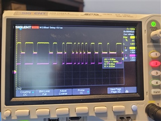
I have attached the CAN waveforms I can see with the EVM.
Thanks,
Priya
Hi Priya,
Thanks for the update and providing the part number for your CAN dongle. It seems like we are making progress. The CAN dongle will certainly throw an error when a CAN FD is on the bus.
Yes, Classical CAN or Standard CAN messages can use either 11-bit or "extended" 29-bit ID's. To use the extended 29-bit ID, the XTD bit in the message header must be set to "1". These messages are limited to a single bit rate less than 2Mbps and a maximum data payload of 8bytes.
The waveforms you provided look correct, have the proper voltage levels, and are of very good quality. They are symmetrical, have a 2.5V recessive level, and little ringing or overshoot. This is what we want to see.
Recall that setting the FDOE and BRSE bits in the CCCR register simply enable the TCAN4550 to be capable of sending and receiving CAN FD messages. However, the FDF, BRS, and DLC bits in the message header determine how the message is transmitted on the bus. Therefore it is possible to send classical (non-FD) messages even with the FDOE and BRSE bits set to "1". The message headers would however require the FDF and BRS bits to be set to "0" to indicate this message is a Classical (non-FD) message.
Regards,
Jonathan
Jonathan,
The TCAN demo project doesn't use the extended 29 bit id and for now I will keep it this way. My current goal is to get a PCAN trace using this CAN dongle.
In the CAN_init routine, I have left the MCAN core settings as:
/* Configure the MCAN core settings */
TCAN4x5x_MCAN_CCCR_Config cccrConfig = {0}; // Remember to initialize to 0, or you'll get random garbage!
cccrConfig.FDOE = 1; // CAN FD mode enable
cccrConfig.BRSE = 1; // CAN FD Bit rate switch enable
Here is the CAN message I am trying to send to the TCAN EVM:
    /* Define the CAN message we want to send*/

    uint8_t data[4] = {0x55, 0x66, 0x77, 0x88};     // Define the data payload
    header.DLC =  MCAN_DLC_4B;                       // Set the DLC to be equal to or less than the data payload (it is ok to pass a 64 byte data array into the WriteTXFIFO function if your DLC is 8 bytes, only the first 8 bytes will be read)
    header.id = 0x52;                              // Set the ID
    header.FDF = 0;                                 // CAN FD frame enabled
    header.BRS = 0;                                 // Bit rate switch enabled
    header.EFC = 0;
    header.MM  = 0;
    header.RTR = 0;
    header.XTD = 0;                                 // We are not using an extended ID in this example
    header.ESI = 0;                                 // Error state indicator


    TCAN4x5x_MCAN_WriteTXBuffer(0, &header, data);  // This function actually writes the header and data payload to the TCAN's MRAM in the specified TX queue number. It returns the bit necessary to write to TXBAR,
                                                    // but does not necessarily require you to use it. In this example, we won't, so that we can send the data queued up at a later point.

    /* Let's make a different CAN message */
    data[0] = 0x11;
    data[1] = 0x22;
    data[2] = 0x33;
    data[3] = 0x44;                                 // Define the data payload

    header.DLC =  MCAN_DLC_4B;                       // Set the DLC to be equal to or less than the data payload (it is ok to pass a 64 byte data array into the WriteTXFIFO function if your DLC is 8 bytes, only the first 8 bytes will be read)
    header.id = 0x123;                              // Set the ID
    header.FDF = 0;                                 // CAN FD frame enabled
    header.BRS = 0;                                 // Bit rate switch enabled
    header.EFC = 0;
    header.MM  = 0;
    header.RTR = 0;
    header.XTD = 0;                                 // We are not using an extended ID in this example
    header.ESI = 0;                                 // Error state indicator
I set both the PCAN analyzer and the TCAN driver project to both have a nominal data sample point of 75% at 500 kbps. I changed the MCAN_Data Timng to:
TCAN4x5x_MCAN_Data_Timing_Simple TCANDataTiming = {0}; // 1 Mbps CAN with a 40 MHz crystal (40E6 / (30 + 10) = 1E6)
TCANDataTiming.DataBitRatePrescaler = 1;
TCANDataTiming.DataTqBeforeSamplePoint = 30;
TCANDataTiming.DataTqAfterSamplePoint = 10;
Please confirm if the TCAN driver settings are correct to transmit regular CAN messages, not CAN FD. The PCAN analyzer connects with status OK and immediately switches to BUSHEAVY status when I run the firmware.
I also tried commenting any message transmit from the firmware. I tried sending a message from the PCAN analyzer. Again, the same BUSHEAVY status. I really need a resolution to this problem.
Hi Priya,
The message information looks good to me for a regular CAN message.
What board are you trying this test on, the TCAN4550 EVM or your custom board? The TCAN4550 EVM has a 40MHz crystal on it, but your custom board has a 20MHz oscillator. Therefore, since you have two different clock frequencies, the TCAN4550 Nominal and Data Bit timing configurations will be different for the two boards.
In Classical CAN there is only a single Nominal bit rate, so the Nominal bit rate settings will be used for the entire message. When the TCAN4550 sees a message header that has the FDF bit set to "0", it should ignore the Data Timing settings and use the Nominal Timing settings for the entire message. Therefore, if you have a Nominal 500kbps configuration, each bit for the message should have a bit width of 2us.
Can you check that you are using the right configuration settings for clock frequency, or verify the bit width on a scope?
You could also set the data timing to match the nominal timing just to make sure there is never a message transmitted at a faster speed. But you shouldn't need to do this.
I don't know if the PCAN analyzer software needs a separate CAN and CAN FD bit timing configuration. The image you showed in a previous post showed both a CAN and a CAN FD tab, so perhaps you could verify this as well.
Regards,
Jonathan
I appreciate the call Jonathan. The CAN trace is now working again with an EVM setup. and I understand the correct scope trigger now. In case complications continue with the custom PCB, I will reach out again. Many thanks!
Hi Priya,
I'm happy to help and I'm glad we were able to get it working!
Regards,
Jonathan