Part Number: TPD4E1U06DBVEVM
I have been reading about protection methods against a static discharge using TVS diodes, and I have a few specific questions still.
- Using the TPD4E1U06DBVR as an example, the Clamping voltage is 15V typical. The graph for a static event is below.
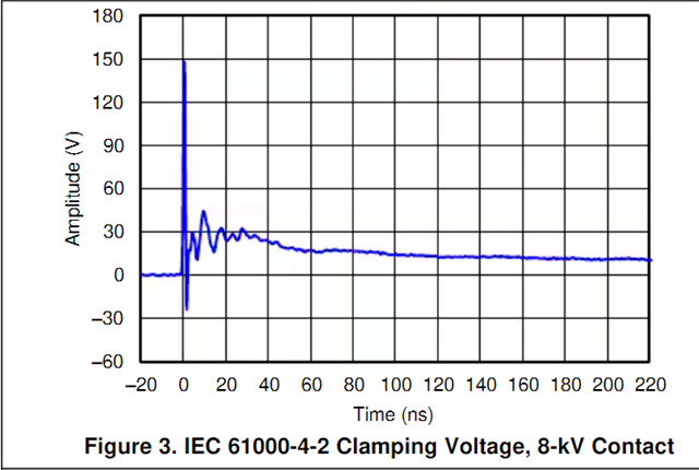
This device is said to be designed for USB 2.0 applications. But most MCUs D+, D- and VUSB power pins can not exceed more than 5V. Or other parts for that matter. It looks like the part will see 15V during the active clamping after the transient. More than 220nS in the graph above. Would that not still damage the part? 15V is quite a bit higher. I would just like some clarification as to why this does not damage parts every time static hits like this. I have read that for protection, you need to choose a clamping voltage that does not exceed the max of the part, but I have a hard time finding a TVS diode that has 5V standoff voltage and has a maximum clamping voltage anywhere near 5 to 6V. Usually much higher like 10-24V. - During the static event, say if it's on an MCU I/O pin. Wouldn't the intrinsic clamping diodes start conducting at some point and cause damage? I assume the TVS protects the input in this case because by the time the body diodes forward bias and start conducting any current high enough to do damage, the TVS would have already absorbed the static event? Is that right?
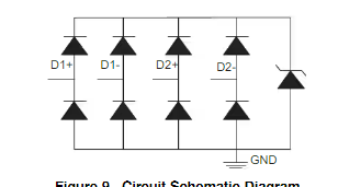
- The block diagram kind of looks like the data lines have standard diode clamping, maybe shottkey diodes, instead of TVS. Since the spec says all pins have a clamping of 15V typ, I am assuming they are all TVS, but the different symbols mean something else? Are the data lines TVS and still have a 15V typ clamping voltage like the graph above?