This thread has been locked.

If you have a related question, please click the "Ask a related question" button in the top right corner. The newly created question will be automatically linked to this question.

SN65DSI84-Q1: Getting the Chip to work on a custom pcb with a embedded display

Part Number: SN65DSI84-Q1
Other Parts Discussed in Thread: DSI-TUNER, SN65DSI86, , SN65DSI85, SN65DSI84, SN65DSI83, SN65DSI83Q1-EVM

Hello everyone,

i already got the display to work with the SN65DSI86, in particular the on the SN65DSI86-EVM thanks to Zach Dryer who pointed out, that i need the excel-sheet for that and that the DSI-Tuner will not work with the Chip.

I got the eDP part working and have to wait for our programmers to get ready to do the MIPI part.

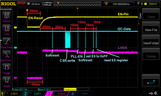
In the meantime i need to test the SN65DSI84-Q1 chip with the display aswell. I made a small pcb with the chip and the chip works and i can access it via i2c. The vcore of 1V is also good.

But i have the same problem with generating the necessery i2c settings as i had with the other chip.

My display has the following edid data, that i read out of a eDP to LVDS chip that works with that display on another pcb:

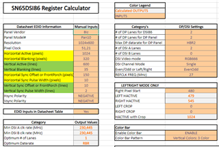
The settings of the excel sheet that i used to get the testpattern to work with the SN65DSI86 are the following:

The DSI-Tuner does not accept horizontal and vertical blanking pixels. It only accepts horizontal and vertical backporch so i calculated the values according to the datasheet of the ic on page 40:

BackPorch = Blanking - (Offset or FrontPorch + PulseWidth)
I got the following values:


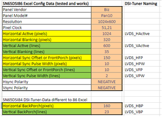
The DSI-Tuner settings are now the following:

My first priority is to get the testpattern to work, so if the MIPI settings are a bit wrong i am okay for the moment.

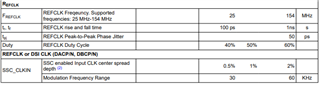
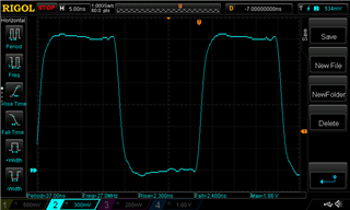
My custom pcb has a 27Mhz oscillator directly connected to the REFCLK input. Because the datasheet of the display specifies a 51.21 Mhz Clock for the display i deemed it okay to use that and use the times two multiplier in the ic. The clock can be between 44,9 and 63 Mhz according to the datasheed of the display.

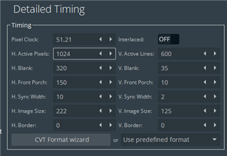
Here are the timing parameters directly from the datasheet of the display:

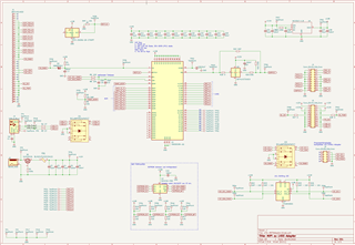
i am thankfull for any ideas. I will post the schematic of the pcb if necessary

Thank you very much,

Marc

  • Hello, Marc,

    Have you tried to display the test generation pattern on a panel? The LVDS parameters in the DSI-Tuner look good.

    Thanks,

    Zach

  • Hello Zach,

    and again thank you verry much for your help.

    The first step i want to try is to get the pattern generation to work.
    I set the 0x3C register to 0x01 but with no luck. Maybe i program it in the wrong order? I just copied the output of the DSI-Tuner and converted it to a format that my I2C Master can read and program. The only changes i did was to add a soft reset first, disabled the PLL, set all the clock settings and enabled the PLL the rest is from the DSI-Tuner.

    Here is the schematic of my pcb maybe there is the issue?

  • Marc,

    Can you verify that you are setting the CHA_TEST_PATTERN = 0x10? 

    I see above that you state 0x3C register to x01.

    Thanks,

    Zach

  • Hello Zach,

    sorry, i misswrote it in my message to you. I programmed the correct value. Here is the ouput from the DSI Tuner with the added soft-reset at the beginning and the disable and enable of the pll before and after clock settings.

    0x09 0x01
    0x0D 0x00
    0x0A 0x02
    0x0B 0x01
    0x0D 0x01
    0x10 0x36
    0x11 0x00
    0x12 0x2f
    0x13 0x00
    0x18 0x70
    0x19 0x00
    0x1A 0x03
    0x1B 0x00
    0x20 0x00
    0x21 0x04
    0x22 0x00
    0x23 0x00
    0x24 0x58
    0x25 0x02
    0x26 0x00
    0x27 0x00
    0x28 0x20
    0x29 0x00
    0x2A 0x00
    0x2B 0x00
    0x2C 0x0a
    0x2D 0x00
    0x2E 0x00
    0x2F 0x00
    0x30 0x02
    0x31 0x00
    0x32 0x00
    0x33 0x00
    0x34 0xa0
    0x35 0x00
    0x36 0x17
    0x37 0x00
    0x38 0x96
    0x39 0x00
    0x3A 0x0a
    0x3B 0x00
    0x3C 0x10
    0x3D 0x00
    0x3E 0x00

  • Hello, Marc,

    I will take a look at all the information you provided above. 

    I see you provided a snippet of the panel's datasheet . However, could you provide the entire panel datasheet for me to review?

    Thanks,

    Zach

  • Hello Zach,

    thank you for your help. The display we use is a topway display. The datasheet cant be found online i will try to get it and will contact you.

    The display is very similar to that one: https://www.topwaydisplay.com/sites/default/files/2020-02/LMT101ENMFWD-NAC.pdf

    I will send you the right datasheet via private message. The parameters i used with the SN65DSI86 that i calculated with the excel sheet worked fine so maybe it is a setup/programming problem? Can i programm the registers in the order i provided above ?

    Thank you verry much for your help.

  • Hello, Marc,

    You need to match your LVDS frequency (nominal) to 54MHz.

    You need to use DSI CLK = (54*18)/(2*2) = 243MHz. 

    Thanks,

    Zach

  • Hello Zach,

    okay thank you, i will change that. But if i use the REFCLK with a oscillator of 27MHz and a PLL Multiplier of 2 i get 54Mhz which should be fine, right?
    And the Testpattern should work without a DSI Input like i did with the SN65DSI86 EVM Board on the other Forum Thread you helped me with.

    Thanks,

    Marc

  • Marc,

    54MHz is within the range of the datasheet and you should be fine.

    Test pattern works without the DSI input that is correct.

    Thanks,

    Zach

  • Okay, so it should work with the settings.

    I just dumped the complete CSR from 0x00 to 0xff and for 0xE5 i got 0x01. For 0xF4 i got 0x40 and for 0xF7 i got 0x80. The Registers above 0xE5 are not specified in the datasheet. Are these special ones? The 0x01 in 0xE5 says it is a PLL_UNLOCK. I just checked the 27MHz clock and it is stable. Is a 1V8 Quarz-Oscillator the correct one? In the EVM-Schematic they use a external PLL/Clock-distributing-IC but i just need the 27Mhz for the 54MHz display. Any ideas?

    The LVDS signal on the display pcb is converted via the GM8284DD IC to RGB Here is the datasheet, unfortunately only in chinese:

    https://datasheet.lcsc.com/lcsc/1809111820_CORPRO-GM8284DD_C245023.pdf

    Thanks,

    Marc

  • Marc,

    Is there a way to troubleshoot by disconnecting the REF_CLOCK and using the internal DSI_CLK for now to see if that gives you a working LVDS display? The internal test pattern although does not use DSI_DATA lanes does use the REF_CLK or DSI_CLK.

    Thanks,

    Zach

  • Hello Zach,

    well i have running code on the RT1170-EVK board that could work with the converter. The problem is, that the code is for the EVK-Display and has completely different specs regarding the frequency, the lanes and so on. I could try it out. Our software development team unfortunately has no time at the moment to implement. Do you see any other error in my schematic or the CSR? I am out of ideas regarding the 84. The 86 works perfectly fine on the evalboard with the 27MHz without the DSI plugged in.

    Thanks,

    Marc

  • Marc,

    Could you verify that you are using DSI-TUNER 2.1?

    Can you use an oscope to see if you are getting LVDS data out of the device?

    If not I have attached it here: 0143.DSI Tuner 2.1.zip

    I will recheck your schematic and CSR.

    Thanks,

    Zach

  • Hello Zach,

    i used the DSI-Tuner 2.0. I downloaded your version 2.1 and will test it out on monday.
    I will try to measure the LVDS output as well.

    Thanks,

    Marc

  • Marc,

    Great to hear let me know if you can get it to work.

    Thanks,

    Zach

  • Hello Zach,

    unfortunately it still does not work with the DSI-Tuner Version 2.1.

    What i dont understand is that the DSI-Tuner sets the reserved bits in some registers.

    For example i got for the CSR 0x10 the value 0x36 which sets reserved values and the register description of the DSI-Tuner does not match the description in the datasheet but it matches the desctiption of the SN65DSI85 datasheet... I chose the SN65DSI84 in the tuner. The values would match the values for the SN65DSI85 might that be a problem?

    Can you tell me what the HS state for the dsi clock and the LP11 state for the datalines mean? Is that necessary for the Testpattern? I still have the DSI inputs not connected and they are just floating. Do i need to ground them or whatever to get the testpattern to work?

    Thanks,

    Marc

  • Hello, Marc,

    I used the DSI-TUNER tool based on the information provided so far.

    Could you verify that your current configuration file is the same?

    //=====================================================================
    // Filename   : CSR_E2E.txt
    //
    //   (C) Copyright 2013 by Texas Instruments Incorporated.
    //   All rights reserved.
    //
    //=====================================================================
    0x09              0x00
    0x0A              0x02
    0x0B              0x00
    0x0D              0x00
    0x10              0x36
    0x11              0x00
    0x12              0x30
    0x13              0x00
    0x18              0x70
    0x19              0x00
    0x1A              0x03
    0x1B              0x00
    0x20              0x00
    0x21              0x04
    0x22              0x00
    0x23              0x00
    0x24              0x58
    0x25              0x02
    0x26              0x00
    0x27              0x00
    0x28              0x20
    0x29              0x00
    0x2A              0x00
    0x2B              0x00
    0x2C              0x0a
    0x2D              0x00
    0x2E              0x00
    0x2F              0x00
    0x30              0x0a
    0x31              0x00
    0x32              0x00
    0x33              0x00
    0x34              0xa0
    0x35              0x00
    0x36              0x17
    0x37              0x00
    0x38              0xa0
    0x39              0x00
    0x3A              0x0c
    0x3B              0x00
    0x3C              0x10
    0x3D              0x00
    0x3E              0x00
    
    
    The PLL_EN bit and SOFT_RESET bit are not set as they need to be set per the recommended sequence defined in the datasheet

    Also, the HS state for the DSI CLK is the High Speed state per the MIPI spec. LP11 is when all DSI DATA lanes are high. 

    Please see this link for some additional detail:

    https://www.edn.com/all-you-need-to-know-about-mipi-dphy-rx/

    Thanks,
    Zach

  • Hello Zach,

    thank you verry much for your help so far.

    I compared your CSR-file with mine and i found 3 differences:

    address: 0x30 (vsync pulse width low) your value 0x0A (int 10), my value 0x02 (int 2)

    address: 0x38 (horizontal front porch) your value 0xA0 (int 160), my value 0x96 (int 150)

    address: 0x3A (vertical front porch) your value 0x0C (int 12), my value 0x0A (int 10)

    can you explain the differences? For example you have for vertical front porch the value 12 is it 10 and 2 added together (v sync offset + vertical sync pulse width)? I used the same values that worked with the excel sheet and the SN65DSI86.

    I tried your CSR-Values but to on avail, still no testpicture. Any other ideas?

    After i programmed the chip i read out the complete CSR here it is:

    Adress 0x0 Value 35
    Adress 0x1 Value 38
    Adress 0x2 Value 49
    Adress 0x3 Value 53
    Adress 0x4 Value 44
    Adress 0x5 Value 20
    Adress 0x6 Value 20
    Adress 0x7 Value 20
    Adress 0x8 Value 01
    Adress 0x9 Value 00
    Adress 0xa Value 82
    Adress 0xb Value 00
    Adress 0xc Value 00
    Adress 0xd Value 01
    Adress 0xe Value 00
    Adress 0xf Value 00
    Adress 0x10 Value 36
    Adress 0x11 Value 00
    Adress 0x12 Value 30
    Adress 0x13 Value 00
    Adress 0x14 Value 00
    Adress 0x15 Value 00
    Adress 0x16 Value 00
    Adress 0x17 Value 00
    Adress 0x18 Value 70
    Adress 0x19 Value 00
    Adress 0x1a Value 03
    Adress 0x1b Value 00
    Adress 0x1c Value 00
    Adress 0x1d Value 00
    Adress 0x1e Value 00
    Adress 0x1f Value 00
    Adress 0x20 Value 00
    Adress 0x21 Value 04
    Adress 0x22 Value 00
    Adress 0x23 Value 00
    Adress 0x24 Value 58
    Adress 0x25 Value 02
    Adress 0x26 Value 00
    Adress 0x27 Value 00
    Adress 0x28 Value 20
    Adress 0x29 Value 00
    Adress 0x2a Value 00
    Adress 0x2b Value 00
    Adress 0x2c Value 0a
    Adress 0x2d Value 00
    Adress 0x2e Value 00
    Adress 0x2f Value 00
    Adress 0x30 Value 0a
    Adress 0x31 Value 00
    Adress 0x32 Value 00
    Adress 0x33 Value 00
    Adress 0x34 Value a0
    Adress 0x35 Value 00
    Adress 0x36 Value 17
    Adress 0x37 Value 00
    Adress 0x38 Value a0
    Adress 0x39 Value 00
    Adress 0x3a Value 0c
    Adress 0x3b Value 00
    Adress 0x3c Value 10
    Adress 0x3d Value 00
    Adress 0x3e Value 00
    Adress 0x3f Value 00
    Adress 0x40 Value 00
    Adress 0x41 Value 00
    Adress 0x42 Value 00
    Adress 0x43 Value 00
    Adress 0x44 Value 00
    Adress 0x45 Value 00
    Adress 0x46 Value 00
    Adress 0x47 Value 00
    Adress 0x48 Value 00
    Adress 0x49 Value 00
    Adress 0x4a Value 00
    Adress 0x4b Value 00
    Adress 0x4c Value 00
    Adress 0x4d Value 00
    Adress 0x4e Value 00
    Adress 0x4f Value 00
    Adress 0x50 Value 00
    Adress 0x51 Value 00
    Adress 0x52 Value 00
    Adress 0x53 Value 00
    Adress 0x54 Value 00
    Adress 0x55 Value 00
    Adress 0x56 Value 00
    Adress 0x57 Value 00
    Adress 0x58 Value 00
    Adress 0x59 Value 00
    Adress 0x5a Value 00
    Adress 0x5b Value 00
    Adress 0x5c Value 00
    Adress 0x5d Value 00
    Adress 0x5e Value 00
    Adress 0x5f Value 00
    Adress 0x60 Value 00
    Adress 0x61 Value 00
    Adress 0x62 Value 00
    Adress 0x63 Value 00
    Adress 0x64 Value 00
    Adress 0x65 Value 00
    Adress 0x66 Value 00
    Adress 0x67 Value 00
    Adress 0x68 Value 00
    Adress 0x69 Value 00
    Adress 0x6a Value 00
    Adress 0x6b Value 00
    Adress 0x6c Value 00
    Adress 0x6d Value 00
    Adress 0x6e Value 00
    Adress 0x6f Value 00
    Adress 0x70 Value 00
    Adress 0x71 Value 00
    Adress 0x72 Value 00
    Adress 0x73 Value 00
    Adress 0x74 Value 00
    Adress 0x75 Value 00
    Adress 0x76 Value 00
    Adress 0x77 Value 00
    Adress 0x78 Value 00
    Adress 0x79 Value 00
    Adress 0x7a Value 00
    Adress 0x7b Value 00
    Adress 0x7c Value 00
    Adress 0x7d Value 00
    Adress 0x7e Value 00
    Adress 0x7f Value 00
    Adress 0x80 Value 00
    Adress 0x81 Value 00
    Adress 0x82 Value 00
    Adress 0x83 Value 00
    Adress 0x84 Value 00
    Adress 0x85 Value 00
    Adress 0x86 Value 00
    Adress 0x87 Value 00
    Adress 0x88 Value 00
    Adress 0x89 Value 00
    Adress 0x8a Value 00
    Adress 0x8b Value 00
    Adress 0x8c Value 00
    Adress 0x8d Value 00
    Adress 0x8e Value 00
    Adress 0x8f Value 00
    Adress 0x90 Value 00
    Adress 0x91 Value 00
    Adress 0x92 Value 00
    Adress 0x93 Value 00
    Adress 0x94 Value 00
    Adress 0x95 Value 00
    Adress 0x96 Value 00
    Adress 0x97 Value 00
    Adress 0x98 Value 00
    Adress 0x99 Value 00
    Adress 0x9a Value 00
    Adress 0x9b Value 00
    Adress 0x9c Value 00
    Adress 0x9d Value 00
    Adress 0x9e Value 00
    Adress 0x9f Value 00
    Adress 0xa0 Value 00
    Adress 0xa1 Value 00
    Adress 0xa2 Value 00
    Adress 0xa3 Value 00
    Adress 0xa4 Value 00
    Adress 0xa5 Value 00
    Adress 0xa6 Value 00
    Adress 0xa7 Value 00
    Adress 0xa8 Value 00
    Adress 0xa9 Value 00
    Adress 0xaa Value 00
    Adress 0xab Value 00
    Adress 0xac Value 00
    Adress 0xad Value 00
    Adress 0xae Value 00
    Adress 0xaf Value 00
    Adress 0xb0 Value 00
    Adress 0xb1 Value 00
    Adress 0xb2 Value 00
    Adress 0xb3 Value 00
    Adress 0xb4 Value 00
    Adress 0xb5 Value 00
    Adress 0xb6 Value 00
    Adress 0xb7 Value 00
    Adress 0xb8 Value 00
    Adress 0xb9 Value 00
    Adress 0xba Value 00
    Adress 0xbb Value 00
    Adress 0xbc Value 00
    Adress 0xbd Value 00
    Adress 0xbe Value 00
    Adress 0xbf Value 00
    Adress 0xc0 Value 00
    Adress 0xc1 Value 00
    Adress 0xc2 Value 00
    Adress 0xc3 Value 00
    Adress 0xc4 Value 00
    Adress 0xc5 Value 00
    Adress 0xc6 Value 00
    Adress 0xc7 Value 00
    Adress 0xc8 Value 00
    Adress 0xc9 Value 00
    Adress 0xca Value 00
    Adress 0xcb Value 00
    Adress 0xcc Value 00
    Adress 0xcd Value 00
    Adress 0xce Value 00
    Adress 0xcf Value 00
    Adress 0xd0 Value 00
    Adress 0xd1 Value 00
    Adress 0xd2 Value 00
    Adress 0xd3 Value 00
    Adress 0xd4 Value 00
    Adress 0xd5 Value 00
    Adress 0xd6 Value 00
    Adress 0xd7 Value 00
    Adress 0xd8 Value 00
    Adress 0xd9 Value 00
    Adress 0xda Value 00
    Adress 0xdb Value 00
    Adress 0xdc Value 00
    Adress 0xdd Value 00
    Adress 0xde Value 00
    Adress 0xdf Value 00
    Adress 0xe0 Value 00
    Adress 0xe1 Value 00
    Adress 0xe2 Value 00
    Adress 0xe3 Value 00
    Adress 0xe4 Value 00
    Adress 0xe5 Value 01
    Adress 0xe6 Value 00
    Adress 0xe7 Value 00
    Adress 0xe8 Value 00
    Adress 0xe9 Value 00
    Adress 0xea Value 00
    Adress 0xeb Value 00
    Adress 0xec Value 00
    Adress 0xed Value 00
    Adress 0xee Value 00
    Adress 0xef Value 00
    Adress 0xf0 Value 00
    Adress 0xf1 Value 00
    Adress 0xf2 Value 00
    Adress 0xf3 Value 00
    Adress 0xf4 Value 40
    Adress 0xf5 Value 00
    Adress 0xf6 Value 00
    Adress 0xf7 Value 80
    Adress 0xf8 Value 00
    Adress 0xf9 Value 00
    Adress 0xfa Value 00
    Adress 0xfb Value 00
    Adress 0xfc Value 00
    Adress 0xfd Value 00
    Adress 0xfe Value 00
    Adress 0xff Value 00

    Here is what i gathered, ignore the 7 inch display for the moment i want to get the 10 inch to work first.

    Thanks,

    Marc

  • Hello, Marc,

    Thank you. Next step could you confirm with a screen capture of your oscope that your initialization sequence is following the correct sequence of events.

    Please see this FAQ for what I am looking for:

    https://e2e.ti.com/support/interface-group/interface/f/interface-forum/852871/faq-sn65dsi84-no-display-output-with-sn65dsi83-sn65dsi84-sn65dsi85

    Thanks,

    Zach

  • Hello Zach,

    okay i will look into the init routine more closely and will get back with a screenshot. Do i just leave the MIPI-Pins unconnected? LP11 state means 1.2V but i dont want to connect it to the RT1170 MCU at the moment for the testpattern. The SN65DSI86 also worked without the MIPI part connected.

    Can you elaborate the differences between our CSR-Registers ?

    I do initialyze it via a Raspberry Pi Pico running micropython and a I2C-lvl-shifter, my code looks like that. Do i write to the registers that have no discription in the datasheet? 

    def initSN65DSI84(i2c,adr):
        print("Writing to adress " + hex(adr) + " ...")
        SN65DSI_enable_pin = machine.Pin(6, machine.Pin.OUT) # pulled up by resistor on pcb, set low to reset
        
        # initialization
        
        SN65DSI_enable_pin.off()					# reset SN65DSI
        time.sleep_ms(25)
        SN65DSI_enable_pin.on()						# enable SN65DSI
        i2c.writeto_mem(0x2c,0x09,bytes([0x00]))	# softreset
        time.sleep_ms(25)
        i2c.writeto_mem(0x2c,0x0D,bytes([0x00]))	# disable pll
        i2c.writeto_mem(0x2c,0x0A,bytes([0x02]))	# LVDS clk range for 54MHz
        i2c.writeto_mem(0x2c,0x0B,bytes([0x02]))	# refclk multiplied by two
        i2c.writeto_mem(0x2c,0x10,bytes([0x10]))	# two DSI lanes
        i2c.writeto_mem(0x2c,0x11,bytes([0x00]))	# no eq
        i2c.writeto_mem(0x2c,0x12,bytes([0x30]))	# dsi clk range between 240 and 245 MHz
        i2c.writeto_mem(0x2c,0x13,bytes([0x00]))	# ----- no register description
        i2c.writeto_mem(0x2c,0x18,bytes([0x70]))	# lvds chan 1 enable, hs and vs neg polarity
        i2c.writeto_mem(0x2c,0x19,bytes([0x00]))	# lvds output voltage
        i2c.writeto_mem(0x2c,0x1A,bytes([0x03]))	# no reverse lvds, 200Ohm termination
        i2c.writeto_mem(0x2c,0x1B,bytes([0x00]))	# no common voltage adjust
        i2c.writeto_mem(0x2c,0x20,bytes([0x00]))	# active line length low
        i2c.writeto_mem(0x2c,0x21,bytes([0x04]))	# active line length high -> 0x0400 -> 1024
        i2c.writeto_mem(0x2c,0x22,bytes([0x00]))	# ----- no register description
        i2c.writeto_mem(0x2c,0x23,bytes([0x00]))	# ----- no register description
        i2c.writeto_mem(0x2c,0x24,bytes([0x58]))	# vertical display size low
        i2c.writeto_mem(0x2c,0x25,bytes([0x02]))	# vertical display size high -> 0x0258 -> 600
        i2c.writeto_mem(0x2c,0x26,bytes([0x00]))	# ----- no register description
        i2c.writeto_mem(0x2c,0x27,bytes([0x00]))	# ----- no register description
        i2c.writeto_mem(0x2c,0x28,bytes([0x20]))	# sync delay low
        i2c.writeto_mem(0x2c,0x29,bytes([0x00]))	# sync delay high -> 0x0020 -> 32
        i2c.writeto_mem(0x2c,0x2A,bytes([0x00]))	# ----- no register description
        i2c.writeto_mem(0x2c,0x2B,bytes([0x00]))	# ----- no register description
        i2c.writeto_mem(0x2c,0x2C,bytes([0x0a]))	# hsync pulse width low
        i2c.writeto_mem(0x2c,0x2D,bytes([0x00]))	# hsync pulse width high -> 0x000a -> 10
        i2c.writeto_mem(0x2c,0x2E,bytes([0x00]))	# ----- no register description
        i2c.writeto_mem(0x2c,0x2F,bytes([0x00]))	# ----- no register description
        i2c.writeto_mem(0x2c,0x30,bytes([0x0a]))	# vync pulse width low
        i2c.writeto_mem(0x2c,0x31,bytes([0x00]))	# vsync pulse width high -> 0x000a -> 10
        i2c.writeto_mem(0x2c,0x32,bytes([0x00]))	# ----- no register description
        i2c.writeto_mem(0x2c,0x33,bytes([0x00]))	# ----- no register description
        i2c.writeto_mem(0x2c,0x34,bytes([0xa0]))	# horizont back porch -> 160
        i2c.writeto_mem(0x2c,0x35,bytes([0x00]))	# ----- no register description
        i2c.writeto_mem(0x2c,0x36,bytes([0x17]))	# vertical back porch -> 23
        i2c.writeto_mem(0x2c,0x37,bytes([0x00]))	# ----- no register description
        i2c.writeto_mem(0x2c,0x38,bytes([0xa0]))	# horizontal front porch -> 160
        i2c.writeto_mem(0x2c,0x39,bytes([0x00]))	# ----- no register description
        i2c.writeto_mem(0x2c,0x3A,bytes([0x0c]))	# vertical front porch -> 12
        i2c.writeto_mem(0x2c,0x3B,bytes([0x00]))	# ----- no register description
        i2c.writeto_mem(0x2c,0x3C,bytes([0x10]))	# test pattern active
        i2c.writeto_mem(0x2c,0x3D,bytes([0x00]))	# ----- no register description
        i2c.writeto_mem(0x2c,0x3E,bytes([0x00]))	# ----- no register description
        time.sleep_ms(25)
        i2c.writeto_mem(0x2c,0x0D,bytes([0x01]))	# enable PLL
        time.sleep_ms(25)
        i2c.writeto_mem(0x2c,0x09,bytes([0x00]))	# softreset

    Thanks,

    Marc

  • Marc,

    You need to follow the entire initialization sequence to ensure proper functionality of the device and get the test pattern. Once you follow the initialization sequence then you can set the register 0x3C to 0x10 and get the test pattern.

    Part of the initialization sequence is: after power is applied and stable, the DSI CLK lanes MUST be in HS state and the DSI data lanes MUST be driven to LP11 state. 

    As for the CSR register differences, I took the typical values for the HFP and VFP from the datasheet you provided. I increased the VSYNC to be more towards the middle range of your datasheet. 

    Thanks,

    Zach

  • Hello Zach,

    so i do have to connect the MIPI Signals to my source even if i only want to use the test pattern? With the SN65DSI86-EVM i just left the MIPI pins unconnected and got the testpattern after is set the CSR. I will look into how i could set the pins to the correct voltage levels. I will rewrite the init with the 0x3C set to 0x10 at the end of the initialization.

    I found this answer from Ikechukwu Anyiam here in the forum which explaines why it worked with the SN65DSI86-EVM. 

    https://e2e.ti.com/support/interface-group/interface/f/interface-forum/991094/sn65dsi84-q1-after-power-is-applied-and-stable-how-can-we-let-the-dsi-clk-lanes-to-be-in-hs-state-and-let-the-dsi-data-lanes-be-driven-to-lp11-state-there-is-anything-we-should-to-do

    Hi Chen,
    
    1. In test pattern mode the device does not use any input DSI data. It only uses the DSI CLK or optionally an external REFCLK. The clock is used to internally generate the pattern and output it to a display
    
    2. Step 2 and step 8 do not need to be followed in test pattern mode
    
    3. You can try this version of the tool instead: https://tidrive.ext.ti.com/u/5B25JYQduSH2Hbkl/DSI%20Tuner%202.1.zip?l 
    
    Regards,
    
    I.K.

    Thank you for clarifying the different CSR values.

    Here is a screencapture. At the moment i am at my homelab with a slower 100Mhz oscilloscope, when i back in the office tomorrow i will capture the lvds with a faster scope because i think i am not able to see data because the sampling rate is to slow. I did not capture the MIPI because it is unconnected. The EN-pin has a litte to high of a capacitance, i think i will reduce the cap at the enable pin, that is why i exceedet the delay everywhere. In the datasheet it is noted, that the delays described there are the minimum and that it is okay to exceed that. I tried it without and with the softreset at the begining after the EN, no change. The value of the 0xE5 after readout is 0x01 so there seems a problem with the PLL (This bit is set whenever the PLL Lock status transitions from LOCK to UNLOCK.)

    Is my schematic with the clock wrong?

    Thanks,

    Marc

  • Marc,

    I will take a look at this and get back to you shortly.

    Thanks,

    Zach

  • Marc, 

    I don't see any obvious problems with the schematic.

    I would like to see scope shots of your DSI- data and the reference clock. What is your rise and fall time on the ref clock?

    Thanks,

    Zach

  • Hello Zach,

    as i mentioned before: There is no DSI-Data and no DSI-Clock i want to get the testpattern to work first without MIPI-Data. We have no working software with the display only with the display that came with the MCU-Devboard which is resolution- and timing-wise far away from the display we want to get to work here.

    The RefClock looks like that:

    There is quite the over and undershoot but that could be the measurement. The probepoint is on the underside and i had to solder a short wire to it to connect the probe. The Oscillator is very close to the IC (around 1cm) The Voltage with the spikes is around 2,6V and 1,875V without the spikes. I am using a hcmos oscillator: ECS-2520Q-18-270DPT is that the wrong oscillator? Do i need a different one with pure sine output? Do i need to terminate the clock in a specific way or just feed the output from the quarz oscillator directly to the ic?

    Thanks,

    Marc

  • Hello, Marc,

    You need to follow the entire initialization sequence to ensure proper functionality of the device and get the test pattern. Once you follow the initialization sequence then you can set the register 0x3C to 0x10 and get the test pattern.

    Additionally, the datasheet specifications on the REFCLK are shown below for the DSI84:


    The rise and fall times you captured surpass the 1ns rise and fall time specified in the DSI84 datasheet.

    Thanks,

    Zach

  • Hello Zach,

    can you explain why i dont have to follow the initialisation with the SN65DSI86? I just left the MIPI interface unconnected there and it worked after i configured the CSR and set the 0x3C register accordingly.

    I got the SN65DSI83 EVM now and measured the refclock pin of this EVM as well as the refclock pin of the SN65DSI86 EVM. Both have rise- and falltime of about 2.4ns. I have not been able to test the 83EVM with the display just yet but the datasheet of the 83 chip also specifies a rise- and falltime of 1ns but TI sells the EVM with the 2,4ns so it should work.

    The picture shows the generated refclk from the output of the CDCEL913PW on the SN65DSI83Q1-EVM.

    Thanks,

    Marc

  • Hello, Marc,

    Since you have the DSI83 EVM, have you tried to configure it in the same way you configure the DSI84 on your board for the test pattern generation case?

    Are you still having the E5 readout as 0x01? Does this happen only with the REF CLK?

    Thanks,

    Zach

  • Hello Zach,

    i just got the DSI83 EVM a couple of days ago. I need to adapt the LVDS output to my display via a separate pcb which is currently in the making. Then i will be able to test it.

    I will only be able to test the testpattern at the moment because i dont have any sourcecode for our MCU to get the MIPI part to work, therefore i can only test it with the refclock and not the MIPI clock, because no MIPI data and clock is available at the time.

    I will get back to you as soon as i have results with the DSI83 EVM.

    Thanks,

    Marc

  • Marc,

    No problem. The EVM will provide a baseline for the DSI84 design.

    Thanks,

    Zach

  • Hello Zach,

    i was looking for the schematic and the board file of the SN65DSI83Q1-EVM, i have the blue version of the PCB. The schematic in the document on the TI-Page with the name: "SN65DSI83, SN65DSI84, and SN65DSI85 EVM User’s Manual and Implementation Guide" is not correct for this PCB version.

    I found this board file which looks like it is the right one:

    https://e2e.ti.com/support/interface-group/interface/f/interface-forum/990796/sn65dsi83q1-evm-needing-to-design-a-daughter-board-around-2-of-the-connectors?tisearch=e2e-sitesearch&keymatch=sn65dsi83q1#

    Could you please verify it and could you please provide me with the schematic aswell.

    To answer your last question: I still got the same error with the E5 readout. I will continue to test it today and give you a overview of my setup.

    Thanks,

    Marc

  • Marc,

    I am looking into this and will get back to you shortly.

    Thanks,

    Zach

  • Marc

    Please see attached DSI85-Q1 schematic.

    int062A-001_SCH.pdf

    Do you know if the GM8284DD has the internal 100ohm loading resistor or require external 100ohm loading resistor at its LVDS input? I can't find this information in its datasheet.

    Thanks

    David

  • Marc,

    Also could you try to program the register Address 0x18 from Value 70 to 50 on your custom board implementation?

    Since this will change the VS from negative polarity setting to positive polarity.

    Thanks,
    Zach

  • Hello David,

    thank you for the schematic. It needs 100ohm loading resistors and these are present on the pcb of the display itself.

    Thanks, I got the display to work now with the testpattern but the MIPI part is not working now.

    Marc

  • Hello Zach,

    sorry that it took me so long to answer. I made some progress and the testpattern works now.

    The problem was a wrongly set clock divider and therefore, for some reason, the PLL did not lock and also there was a problem on the display pcb itself with a special port that needs to be enabled.
    The MIPI part was still unconnected, so as i suspected the problem was not the missing MIPI-Input or wrong MIPI-States, but a clock problem.
    Now i can turn the testpattern on and off and the display works correctly. I tested both the 83EVM and my 84Adapter both work now with the CSR.
    But i still cant get the MIPI part to work. I have a different MIPI to LVDS Adapter with the name GM8775C and that one works flawlessly now.
    The RT1170 NXP board just puts out the framebuffer and the GM8775C accepts the data. That chip has a external eeprom with the edid data of the display and it does not need to be programmed via I2C after powerup.
    So the MIPI signals are good but the 83 and 84 dont work. Sometimes i get a CHA_SYNCH_ERR error in the 0xE5 register. Any ideas?

    Thanks,
    Marc

  • Marc

    Can you please measure the line time on the MIPI side to verify it is meeting the LVDS timing requirement?

    Please see this e2e guide on how to measure the line time on the MIPI DSI input, https://e2e.ti.com/support/interface-group/interface/f/interface-forum/852871/faq-sn65dsi84-no-display-output-with-sn65dsi83-sn65dsi84-sn65dsi85.

    Thanks

    David

  • Hello David,

    i can do that but i would say the timing is good because the same display with the same data from our RT1170 EVK works with the GM8775C no problem and i get a perfect picture. On the display is a adapter with the GM8775C chip and we need to make a alternative board for that and that one works with the display no problem. We entered the display parameters directly in code and used the parameters calculated by the dsi tuner fot the generation of the displaydata from the rt1170 so i would say that it should work. I will measure the MIPI to see if there is another problem or if the 83EVM has a problem..

    Thanks

    Marc

  • A quick followup:

    i read out the 0xE5 register and got all errors except for the PLL unlock (i derive the clock from the 27Mhz Oscillator on the board and multiply that by two, should i use the mipi clock instead ?) the 0xE5 register value is 0xFC.

    Thanks

    Marc

  • Hello,

    Are you following the initialization sequence per the datasheet?

    Thanks,
    Zach

  • Hello Zach,

    i got the display to work with the 84-Adapter that i build and the 83-EVM. The problem was not the initialisation. The initialisation doesnt really matter: You can turn the source on and stream video and after that turn on the EVM or Adapter and and set the registers and it starts working. Putting the MIPI in the "idle" states and doing the initialisation is not really necessary.

    One very anoying "problem" i found out is that in the datasheet some registers are descibed as "reserved" and "do not write to that register" but the CSR generated from the DSI-Tuner will write to these registers and when you look into the register description in the DSI Tuner these registers are not "reserved". Why is that so ? It is realy anoying to work with these inconsistencies. The register DSI_CHANNEL_MODE in 0x10 is not described at all for example in the datasheet, it is not known what value to put there. Is it possible to update the datasheets? And also remove the SN65DSI86 entry from the DSI Tuner if only the excel-sheet works?

    I will test a different display now with the three ICs.

    Thanks,

    Marc

  • Hello, Marc,

    Thanks for letting me know about your suggestions.

    I am glad you got the display to work with the EVM and your adapter.

    Thanks,

    Zach

  • Hello Zach,

    so i got all the displays to work with the SN65DSI86 / 84 and 83 ICs to work.

    Thanks for the help.

    Here are a couple of tips for everyone trying the same:

    Create a excel sheet with all the important registers from the datasheet AND the DSI-Tuner and verify that you set them correctly. Some registers are described as reserved in the datasheet but the DSI-Tuner will write to those.

    Start with the testpattern first and completely ignore the the MIPI-Part just leave the MIPI unconnected and the MIPI-Part of the initialisation does not matter at all. You will need a external clock source like a 25MHz Crystal-Oscillator so maybe add one for debugging and later remove it if you plan on using the clock provided by MIPI but you need different clock settings for multiplication and division if you switch from MIPI-Clock to Crystall and vice versa. You will be able to verify that the LVDS or Displayport-Part works before you hassle with the MIPI-Part.

    If you know, that your MIPI-Data is good because you tested it with a different IC and the testpattern works from the SN65DSIxx, you might have a problem with the MIPI-Settings like clock, or the lanes.

    Good luck to everyone

  • Marc,

    You are welcome. Thanks for leaving some lessons learned in this thread.

    Best,

    Zach