


Hi,
in an existing design I need to replace a SN75DP139RGZ with and SN75DP149RSB. Space-wise this is not an issue, also the answer given here
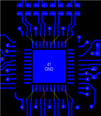
helped me, to arrange the TMDS lanes in a proper way. However, one issue/questions still remains: Is it possible to swap P and N on bot sides, input and out output, in order to facilitate routing even more. Please see attached picture for clarification:
I do not want to change the phase relation between input and output, thus the polarity swap option in redriver mode is not working here.
Short: may I swap P and an at input or output or will this disturb the internal circuits of the IC?
Thank you very much for your support!
Best Regards,
Sebastian
