This thread has been locked.

If you have a related question, please click the "Ask a related question" button in the top right corner. The newly created question will be automatically linked to this question.

TFP401A: Signal Inaccurate - Causing monitor to display Distorted Image

Part Number: TFP401A
Other Parts Discussed in Thread: DS90C387, TFP401

Hello,

Im developing a HDMI to LVDS bridge using TFP401APZP with DS90C387VJDX/NOPB - This is a dual channel converter - I have already asked for help under part number DS90C387 and was told that i wont get any help as the issue is caused by TFP401A.

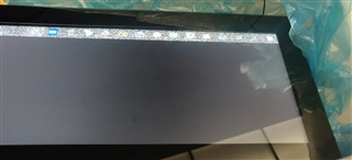
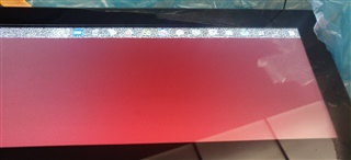
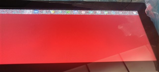
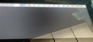
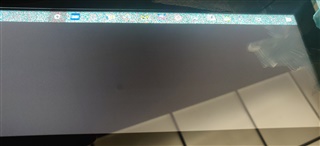
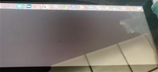
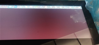
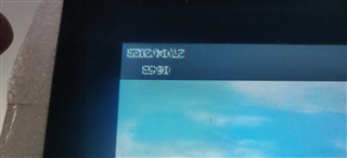
I am experiencing an issue with the display showing a distorted image.

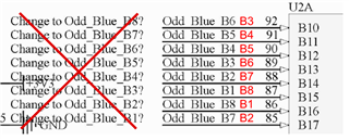
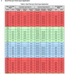
I have attached the previous thread where i have outlined everything i have tried and the current configuration of the system. I have also attached images outlining the issues.

e2e.ti.com/.../4579586

We have tried changing the configuration pins on both TFP401APZP and DS90C387VJDX/NOPB with no change in display or the display stopping completely.

We have chekced the differential pair impedance matching and length matching and chekced the length matching in the RGB outputs.

We have also tried to change the EDID but this either makes no difference or makes the display stop working.

Could you please help us with finding out what could be causing the issue, We would greatly ppreciate it.

Best Regards,

Kacper

00 FF FF FF FF FF FF 00 
1D 85 01 24 01 00 00 00 
20 12 01 04 A1 2B 1B 6D 
EF C5 C6 A3 57 4A 9C 23 
12 4F 54 00 00 00 01 00 
01 00 01 00 01 00 01 00 
01 00 01 01 01 01 30 2A 
80 18 71 68 8E 11 12 20 
0A 08 40 6C 20 00 00 3E 
00 00 00 FF 00 35 31 36 
38 0A 20 20 20 20 20 20 
20 20 00 00 00 FA 00 09 
4F 01 00 01 00 01 00 01 
00 01 00 0A 00 00 00 FC 
00 4C 43 44 20 4D 4F 4E 
49 54 4F 52 20 20 01 29 
02 01 04 00 02 3A 80 18 
71 38 2D 40 58 2C 45 00 
D7 40 32 00 00 1E 01 1D 
00 72 51 D0 1E 20 6E 28 
55 00 D7 40 32 00 00 1E 
01 1D 80 18 71 1C 16 20 
58 2C 25 00 D7 40 32 00 
00 9E 00 00 00 00 00 00 
00 00 00 00 00 00 00 00 
00 00 00 00 00 00 00 00 
00 00 00 00 00 00 00 00 
00 00 00 00 00 00 00 00 
00 00 00 00 00 00 00 00 
00 00 00 00 00 00 00 00 
00 00 00 00 00 00 00 00 
00 00 00 00 00 00 00 95

0724.P19 TFT.pdf

  • Kacper

    Can you share your schematic and layout for this design? 

    Which resolution are you using right now? Is it possible to reduce the resolution and see if the distorted image goes away? 

    Also, when you sent the video from the source, are you including audio as well? The TFP401A only supports video, it can't support audio.

    Thanks

    David

  • Hi David,

    Thank you for your response. 

    I have attached the schematic, but will send the layout when I am back in the office.

    The TFT resolution is 1920 X 360 + blanking pixels. I have tried many different resolutions and only 1080p seems to work but is also distorted. 

    I tried changing the clock frequency (this changed nothing), I suspect adding additional blanking pixels may have an effect, however I'm unsure what values to use as the EDID we are using was taken directly from a dedicated driver board for this specific TFT.

    When audio was included in the signal, the TFT went into diagnostic mode, refusing to work properly. When all audio was removed from the EDID we started receiving the distorted image we are seeing now? Is there anything else that could be causing the issue in the EDID?

    Thank you for your help, I really appreciate your help with the issue.

    Best Regards

    Kacper

    8117.Schematic (1).pdf

  • Kacper

    I am having question on the odd/even pixel connection between TFP401A and DS90C387, and am asking the FPDLink to double it check for me.

    Thanks

    David

  • Hello,

    From even/odd perspective, this looks correct in schematic. However, it looks like the LSB/MSB might be flipped.  The below table/bit orientation will output VESA mode that this panel is targeting. 

    Is TFP401 configured to flip LSB/MSB, or could that be the issue?

    Kacper, can you try a solid red, green, or blue image to see if that displays properly? In this case, I don't think a a LSB/MSB would have impact on the image output.

    Regards, 

    Logan

  • Hi Logan,

    I have tried the Pure blue, red and green outputs on a different thread, I supplied this at the beginning of this thread so please use this as reference for everything I've already tried.

    https://e2e.ti.com/support/interface-group/interface/f/interface-forum/1213055/ds90c387-signal-timing-inaccurate---causing-monitor-to-enter-diagnostics-mode#4579586

    From these tests it seems that pure blue, red and green works correctly, but a colour that requires a combination of RGB doesn't respond properly. 

    How certain are you that it's the MSB and LSB being swapped? - if this is definitely the case then we will try again with a redesigned board. However I want to be as certain as possible before wasting another 1-2 weeks on manufacture. 

    I appreciate your help,

    Best regards

    Kacper

  • Hello, 

    Since today is a US public holiday, we will continue support on your request on Monday. Thank you for your patience. 

    Regards, 

    Logan

  • Okay, thank you.

    I have checked the connections also on the schematic and it agrees with both datasheets for the TFP401APZP and DS90C387VJDX/NOPB.

    I carried out some additional testing with the solid RGB colours to try and understand what is happening:

    I received the following results:

    (0,0,0) RGB always resulted in a Black (No colour) display .

     - First it tested the RED idividual bit values (1, 2, 4, 8. 16. 32. 64. 128)

    Red Bit Value 1 - I expected it to result in no colour change and remain Black, however there is a visible red colour.

    Red Bit Value 2 - I expected it to result in no colour change and remain Black, however there is a visible red colour thats even brighter than Bit value 1.

    Red Bit Value 4

    Red Bit Value 8, 16, 32 all appear black and i have attached 32 as a reference

    Red Bit Value 64

    Red Bit Value 128

    From the Above Results it seems to be that the bits are in the wrong order where bits 1 and 2 are actually the 2 MSB (this is also the case for Green and Blue bits). Can you please explain where the error could be, I have checked the datasheets multiple times and all connections of the data bits seem correct.

    Thank you and Best Regards,

    Kacper

  • Hello Logan and David,

    Could any of you explain why im experiencing the behaviour above, and provide a solution please?

    Best Regards,

    Kacper

  • Kacper

    Please see the pin definition and Table 9-1 which shows for example, RGB7 is on QD23 and QE23.

    Is it possible to change the red pixel ordering on the PCB using blue wire and repeat the solid red color experiment?

    Thanks

    David

  • Hi David,

    Thank you for your message.

    Im pretty certain that the RGB outputs from the TFP401A are correct. Im convinced the error is caused by incorrect RGB connections to the DS90C387VJDX/NOPB.

    I have tried to alter the Red connections using wire but the soldering/length matching inaccuracies caused me to get 'striping' on the screen and some channels were not being received correctly.

    What i did instead is test each bit in the 8-bit Red value to see which is least and most significant in order.

    What i found was the following (Even_Red Channel used as example):

    R20(Pin 84) = R0 LSB

    R21(Pin 81) = R1

    R22(Pin 80) = R2

    R23(Pin 79) = R3

    R24(Pin 78) = R4

    R25(Pin 77) = R5

    R26(Pin 76) = R6

    R27(Pin 75) = R7 MSB

    This seemed to agree for all Even/Odd Green, Blue and Red Data although it was difficult to tell at low RGB values (<32) because the screen appeared almost black.

    Can you confirm that these are the correct connections so that we can get a working PCB manufactured please.

    I have attached the schematic with text explaining the changed connections for reference.

    I also found a document that would agree with my new connections but i think disagrees with the DS90C387VJDX/NOPB datasheet?

    https://www.hobbielektronika.hu/forum/getfile.php?id=164305

    Thank you and Best Regards,

    Kacper

    Annotated Schematic.pdf

  • Kacper, 

    If the display panel RX format requirement is dual OLDI/LVDS VESA format then the following document will help map the inputs of the 387 (see 387 TX column below) https://www.ti.com/lit/an/snla014a/snla014a.pdf

    Your revised annotations still look incorrect. You need to directly mirror the LSB and MSB. Again, this is assuming conventional VESA formatting; you would need to verify this in display.

    Note* this app note and datasheet are indexed from 0-7 instead of 1-8 like your schematic.

    Regards, 

    Logan

  • I dont belive these new connections can be correct based off of the very first set of tests carried out using the Red channel. What we proved was that R17 and R27 were the most significant bits. - This was tested by setting red value to 2, which set Red_B7 (odd & even) high. Setting R16 and R26 resulted in the halving of the Red intensity, it halved again when R15 and R25 are set etc...

    I dont understand how you can tell me that B16 is the most significant bit when my tests show otherwise.

    I also dont understand how you can justify the order of bits when, again, my tests show otherwise.

    From my testing, the crossed out changed below seem to be correct, and I ask if you can please confirm this and not base your responses on the datasheet alone. I also ask you to do this because i have attached a seperate TI document previously which disagrees with the connections. I have copied it below again, please take a look.

    www.hobbielektronika.hu/.../getfile.php

    /resized-image/__size/320x240/__key/communityserver-discussions-components-files/138/pastedimage1681507733193v3.png

    (Blue_B8 = LSB, Blue_B1 = MSB)

    I look forward to hearing from you about whether you've been able to replicate this issue. We are planning to buy hundreds of these chips a year but it seems that we may have to look for a different solution with another manufacturer soon based on the lack of genuine support from TI.

    Best Regards,

    Kacper

  • Kacper,

    Please clarify if display uses JIEDA (format 1) or VESA (format 2) color packing convention for input of display? I do not see it called out in the display datasheet, and this will impact the color mapping requirements in the device. Since TI is not owner of this device, we can not confirm.

    I dont belive these new connections can be correct based off of the very first set of tests carried out using the Red channel.

    An important distinction I now notice that I didn't before is that the the MSB to LSB flip/flop is actually already being done with the signal names/connections at the output of TFP401A. QE0 is the LSB, QE7 is the MSB. But then you are reassigning QE0 to Even_Blue_B8. So the LSB/MSB consideration at the 387 pin naming is inverse. Therefore, the mark-up above where I asked for LSB/MSB to be flipped is actually how it is currently routed.

    Given the above point, I think the issue here is again the JEIDA vs. VESA mapping format.

    Bit 0 in JEIDA format corresponds to bit 6 in VESA.

    Bit 1 in JIEDA format corresponds to bit 7 (MSB) in VESA. This is why "2" was the brightest in your testing.

    The differences in routing between the datasheet and the application note you provided is VESA vs. JEIDA.

    Datasheet mapping table is actually for JEIDA mapping (as shown in above two pictures both taken from datasheet).

    My suspicion is that your panel requires VESA format. The other app note link you listed is for VESA.

    Therefore the routing will need to be modified to match the app note you linked. The crossed out mapping above still seems incorrect though, the MSB/LSB would need swapped since the QE to signal mapping swaps LSB/MSB as mentioned above.

    QE[23] maps to R27

    ..

    QE[16] maps to R20

    I believe this clears things up, but let us know if there are any further questions.

    Regards,

    Logan

  • Hi Logan,

    Thank you for your response, we have since built a new PCB with the changed connections and have a working display.

    There is one final issue that i cant seem to locate. It seems that interlaced pixels are offset by 1 somehow, im not sure how else to describe this.

    I have tried multiple different combinations of settings pins on the hardware, and have also tried everything related to interlacing on the EDID.

    Can you please suggest what could be causing this, either in the hardware or EDID?

    I have attached images of the pixel offset below:

    Could swapping the LVDS channels solve the issue? Swapping A0P - A3P to be the even data, and A4P - A7P to be the odd?

    I look forward to hearing from you,

    Regards,

    Kacper

  • Hi Logan, David,

    After swapping the LVDS Odd/Even outputs the display now works correctly.

    Thank you for all your patience and help with my issue, i really appreciate it.

    Very Best Regards,

    Kacper