This thread has been locked.

If you have a related question, please click the "Ask a related question" button in the top right corner. The newly created question will be automatically linked to this question.

DS90LV031A: Block diagram

Part Number: DS90LV031A
Other Parts Discussed in Thread: DS90LV032A, SN65LVDS31, SN65LVDS32

Hi team,

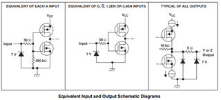
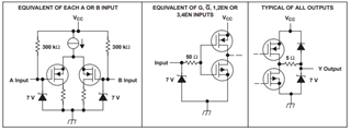
My customer is considering DS90LV031A and DS90LV032A, he wants to know the internal block diagram, could you please provide?

It is possible that the I/O pins may have signals when power off, so he needs to check if it will be a problem.

Additionally, do you have the Pin FMEA report of these devices?

Best,
Zeming 

  • Hello Zeming,

    Unfortunately, we don't have the internal block diagrams for these parts. The closest thing we have is the schematic I/O diagrams. The below are taken from the SN65LVDS31 and SN65LVDS32 but follows a similar structure.

    SN65LVDS31 (LVDS Driver)

    SN65LVDS32 (LVDS Receiver)

    No, the I/Os cannot output signal when the device is powered off. I could not find any FMEA for both DS90LV031A and DS90LV032A.

    Regards,

    Josh