HI.experts
The project is planned to be designed using the TCA9535 and is expected to use 8 TCA9535s.I read the technical manual (SLVA689).There are some questions in the documentation, please help with them.
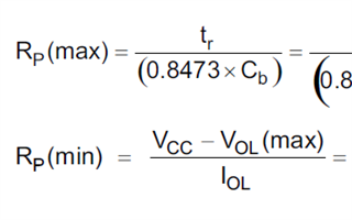
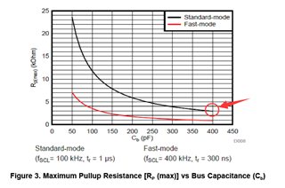
1、How is the value of bus capacitance Cb determined in the manual?
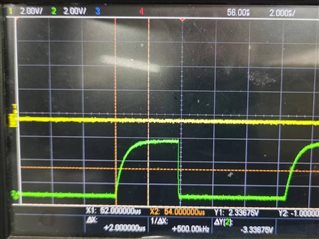
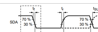
2、In SLVA689 fSCL=100kHZ,Tr=1us,fSCL=400kHZ,Tr=300ns,if fSCL is other frequency how to determine the value of Tr? For example, fSCL=10kHZ, Tr is equal to?
3、If I use 8 TCA9535s, is it ok to use 1 pull-up resistor each for SDA and SCL? Or do I need to use more than one pull-up resistor? What is the proper placement of the pull-up resistors when performing PCBLAOUT?
thank you.