This thread has been locked.

If you have a related question, please click the "Ask a related question" button in the top right corner. The newly created question will be automatically linked to this question.

TPD1E10B06-Q1: TPD1E10B06-Q1 APPLICATION QUESTION

Part Number: TPD1E10B06-Q1
Other Parts Discussed in Thread: ESD2CAN24

Hi team,

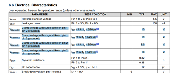
When I learned TPD1E10B06-Q1 DS, I found that the SPEC is related to the test method. could you pls help confirm the following question.

1. Does TI’s bidirectional ESD have polarity?

2. Why do different test methods have different Vclamp and what does this relate to?

Thanks

Hangjie

  • Hi Hangjie,

    I am not certain what you mean by your first question, could you please clarify? If TI states a diode is "Bi-directional," this means the diode will protect against voltage transients in both the positive and negative directions. If TI states a diode is "Uni-directional," this diode will only protect against voltage transients in the positive direction.

    In regards to your second question, the clamping voltage is specified in two different ways here. There is the different directions (one is forward biased, the other is reverse biased), and the other is the Ipp value the clamping voltage was sampled at. This will show the voltage that the diode will clamp at with different surges. This value needs to be less than or equal to the absolute maximum voltage allowed by the downstream circuitry.

    Please let me know if there are any additional questions!

    Best Regards,

    Josh Prushing

  • Hi Prushing,

    Thanks for your support,

    The first question is to confirm whether Pin1 and Pin2 can change directions at will.

    Another question is to confirm whether reducing the parallel capacitance value in the system can amplify the limit value of the ESD device parasitic capacitance, the following is the application of ESD2CAN24, thanks.

  • Hi Hangjie,

    According to the TPD1E10B06-Q1 datasheet, these are the hookup instructions:

    This means as long as one pin is connected to the I/O and the other is connected to GND, the device has been connected correctly. If you would like more information on how the Bi-directional configuration works, please read through Section 2.1 of the following document: TVS3300 Bidirectional Characterization. Although it is for a different device, it describes a bi-directional device's layout in a clear and efficient manner.

    In regard to your second question, I am not certain if I am correctly understanding. Are you asking how to increase the device's maximum capacitance, or are you looking to reduce the total capacitance on the lines with the diode?

    Best Regards,

    Josh Prushing