This thread has been locked.

If you have a related question, please click the "Ask a related question" button in the top right corner. The newly created question will be automatically linked to this question.

TCA9511A: How series and parallel use TCA9511A ?

Part Number: TCA9511A
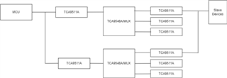
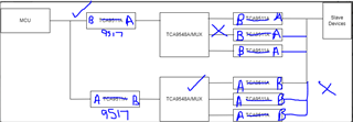
Other Parts Discussed in Thread: TCA9548A, TCA9517, , TCA9517A

Hello, I need to create such an architecture. I thought of using TCA9517 to use buffer, but I find it difficult to connect only the A sides together. For example, the input and output of TCA9548A have to be B side. In this case, it is not recommended for TCA9517.
I am thinking of using TCA9511A, but is it healthy to connect its two OUT outputs together? Or I'm open to Buffer architecture suggestions for this architecture. I'm looking for an IC that can be a parallel node on both sides. Can you help me ?

  • Hi Defne,

    Hello, I need to create such an architecture. I thought of using TCA9517 to use buffer, but I find it difficult to connect only the A sides together. For example, the input and output of TCA9548A have to be B side. In this case, it is not recommended for TCA9517.

    In parallel configurations for the TCA9517, acceptable connections are A-B, B-A, and AA. Only B to B connections are not allowed in a parallel configuration, otherwise, 2 x TCA9517's can be connected to a common node. 

    I am thinking of using TCA9511A, but is it healthy to connect its two OUT outputs together? Or I'm open to Buffer architecture suggestions for this architecture. I'm looking for an IC that can be a parallel node on both sides. Can you help me ?

    For the TCA9511A application, careful consideration must take place when using these devices with RTA's in parallel. I don't see significant offset voltage from the MCU to the TCA9511A since there isn't another switching device or some passive element between the 9511A and MCU that could add to VOL. What we want to avoid is a higher VOL near the ~0.6V trigger threshold of the RTA's that could potentially cause a false trigger of the RTA due to VOL being too high of a voltage plus excessive noise added to the VOL voltage. The parallel TCA9511A would work, but I would see if my suggestions to the TCA9517A can work firstly. 

    Also since a TCA9548A switch is being used in between, the two TCA9511A buffers, we can expect offset voltages to stack. This means that a low generated by the MCU, might appear at a higher voltage when it reaches the slave/target device. 

    The spec Vos is the offset voltage (input-output). It has a maximum of 100mV. This means if the VOL(mcu) = 0.1V, then the output of the TCA9511A would yield VOL(mcu) + 100mV = 0.2V at the output of the first TCA9511A. Add in more voltage from the RDS_ON of the TCA9548A when enabled, + 100mV offset from the 2nd TCA9511A. The voltage seen at the slave/target device might be well into the 0.4 V - 0.5 V range which may more may not be close to the maximum VIL allowed. Say the slave/target device is using 1.8V logic, the maximum low input signal required by the I2C standard would be VIL(max) = 30% of VCC = 0.30 x 1.8V = 0.54V. The voltage might be too close to the maximum VIL due to the various offsets from the output of MCU to the input of the slave device. 

    I tried the multiple TCA9517A's. 

    I see the general issue with B-sides connecting to each other. There really is no good way to connect multiple TCA9517A's together with B-sides connected together. The only way to be able to have this configuration work that I have drawn here is to individual Enable and disable TCA9517A's when the B-sides are connected together. No two TCA9517A's with B-sides connected together can be turned on at the same time. They would have to be addressed separately. 

    May I ask what use case this is going into? Why is there a need for an I2C switch such as the TCA9548A if the end goal is to reconnect them at the end to the same slave device? 

    Regards,

    Tyler