This thread has been locked.

If you have a related question, please click the "Ask a related question" button in the top right corner. The newly created question will be automatically linked to this question.

DP83826E: Schematic review about DP83826

Part Number: DP83826E
Other Parts Discussed in Thread: AM2432

Hi Team,

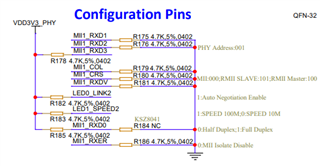
This is customer first design in AM2432+DP83826.

Please help to review the design. Focusing on cheching the interface/config/clock. There are 2 MII network ports and 2RMII slave network ports.

 5383.AM2432-DP83826.pdf

  • Hi Minghao,

    Could you ask the customer to fill out our schematic checklist? Once filled out please return to me and I can review it (will take at most 1 business week). 

    8484.DP83826_Schematic_Design_Review_Checklist.xlsx

    Regards,

    Alvaro

  • Hi Reyes,

    This is my customer feedback.

    Please help about this schematic review.

    7002.DP83826_Schematic_Design_Review_Checklist.xlsx

  • Thank you Minghao,

    I will have the review done by no later than Tuesday 11/21

    Regards,

    Alvaro

  • Hi Minghao,

    I see there are 4 PHYs here to review, I did not do a full schematic review, I only looked at the strapping and clock. I will provide Comments below based off their labeling in the schematic. Attached is the Schematic Checklist with remarks, I only checked D11. Please let me know if there is anything else that you want me to look at.

    DP83826_Schematic_Checklist_D11.xlsx

    All 4 PHYs are configured in BASIC MODE

    All Strap

    • Pull Up Resistors should be 2.2 kΩ
    • Pull Down Resistors should be 1.5 kΩ

    _____________________________________________________________________________________________________________

    D11: 

    PHY ID  001, strapped correctly

    COL & RX_DV pulled high, RMII_SLAVE enabled.

    XI is receiving 50 MHz CLK, this is correct for RMII_SLAVE 

    _____________________________________________________________________________________________________________

    D13:

    PHY ID 010, strapped correctly

    COL & RX_DV is pulled high, RMII_SLAVE enabled.

    XI is receiving 50 MHz CLK, this is correct for RMII_SLAVE 

    _____________________________________________________________________________________________________________

    D15:

    PHY ID 001, strapped correctly, but this is the same PHY_ID as D11, this may cause issues in your system if they are both connected to the same SoC.

    COL & RX_DV are pulled low, MII Enable.

    XI is receiving 25 MHz CLK, this is correct for MII

    _____________________________________________________________________________________________________________

    D17:

    PHY ID 010, strapped correctly, but this is the same PHY_ID as D13, this may cause issues in your system if they are both connected to the same SoC

    COL & RX_DV are pulled high, RMII Slave Mode

    XI is receiving 50 MHz CLK, this is correct for RMII Slave Mode

    Regards,

    Alvaro