This thread has been locked.

If you have a related question, please click the "Ask a related question" button in the top right corner. The newly created question will be automatically linked to this question.

SN75LBC184: LBC184

Part Number: SN75LBC184
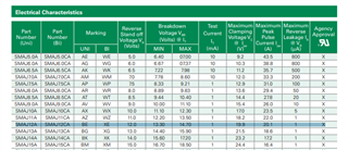
Other Parts Discussed in Thread: THVD1419, THVD1439, THVD2410

Dear Team,

currently we are having issue in the RS485 driver. in our project the driver is failing in our lab.  we are not able to find when the driver fails.

Observation as below : -

when master transmits the voltage levels are different from the voltage levels of receiver sending data, please refer fig 1. the circle highlighted is master transmitting and the rest is receiver sending the response. 

 Fig 1:-

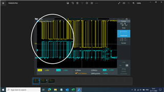
  1. communication was working but there was a difference in voltage.
  2. Initially you see master transmitting highlighted in circle, the potential difference for line A and B seems equal , and then when slave responding the difference is somewhat different.
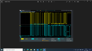
 

In attached Fig 2 :-


  1. Since there was a change in receiver voltage , we change the receiver driver to a new one and then voltage was similar to master. Could you please confirm fig2 is ok?

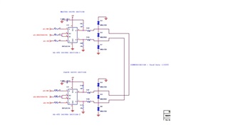
please find attached schematics as ref our design.

Also for your information we are using a pull up and pull down resistor of 10k value. please suggest us is it ok?

thanks and Regards,

Ramdas

  • Please note that the fail-safe (pull-up/-down) resistors are needed only at one place on the bus.

    There are no termination resistors (typically, 120 Ω between A/B at both ends of the bus), but this does not matter for very slow speeds.

    This indeed looks as if the device was damaged. I would guess this is caused by overvoltage, but you already have protection. What kind of noise is there in your environment? Is it possible for the signal lines to be shorted to some other voltage?
    (What matters for RS-485 communication is the differential voltage; tell the oscilloscope to compute A−B.)

  • Hi, 

    Thanks for your quick response.

    By the way do we need pull up /pull down? can i remove it ?

    in case if you say we need pull up and pull down per bus , I will follow the pull up ,pull down for one bus. in that case please could suggest us a value for the pull up and pull down resistors.

    thanks in advance for your reply.

    best regards,

    Ramdas

  • You need fail-safe resistors on the bus if there is at least one receiver without fail-safe input. The SN75LBC184 does not have fail-safe inputs. (Consider a more modern device like the THVD1419/THVD1439.)

    The fail-safe resistors must be able to generate a high enough voltage drop over the termination resistors. Without termination resistors, 10 kΩ is OK.

  • Hi Ramdas,

    Can you please confirm what diode part numbers are being used - I can't make them out in the picture? 

    Also what levels of surge are you trying to protect against? 

    It seems there could be some damage - communication is okay because the differential voltage looks okay; however it could indicate an issue. Did this circuit experience some type of fault event? 

    Please let me know as from an architecture point of view the biggest issue is that there is no termination between A and B on the first/last node - but your signal doesn't look too messy so I don't think that is that big of a deal. There could be protection level mismatches on external protection + internal protection + fault condition experienced. So if you could also confirm if this went under a surge (even if there is a chance that it happened) and what level you are trying to protect against. 

    Best,

    Parker Dodson

  • Hi Parker Dodson,

    thanks for your email. 

    we are using two types of protection one is between terminals, one is (A  to circuit ground, B to circuit ground) and another one is across A and B terminal.

    both A to ground and B to ground are SMAJ12CA (bidirectional TVS) please refer the blow fig1. in case if you cannot find it in the fig please refer datasheet.

    https://www.mouser.in/datasheet/2/240/Littelfuse_TVS-Diode_SMAJ-23503.pdf

    For across A and B we use SMBJ30CA (bidirectional TVS) as in the fig below. please refer datasheet in the below link

    https://www.mouser.in/datasheet/2/240/media-3319099.pdf

    please confirm us on the pull up  pull down values can be 10K.

    thanks and regards,

    Ramdas

  • Hi Ramdas,

    Thanks for the additional information. 

    So I guess that leads me to another question - what surge level are you trying to protect against? 

    I am asking because usually we don't see a device with integrated surge protection paired with additional external surge protection (not that you can't do that - it is okay to do - we just don't see that pairing too often). That being said - depending on surge requirements what might be better is to use a transceiver that has a wider input range. I.e. something like the THVD2410 - which can tolerate up to +/-70V on its inputs. Its not directly surge rated - but depending on the surge rating you would need in your system - you already do have external protection for surge. The benefit of doing something like this is two fold - the first is is that if you are using the surge diodes to protect against power to bus shorts - but the power rail is below 70V you wouldn't actually need the surge diode because the transceiver would be protected and the second benefit would be that if the surge diodes are still required you can usually pick a higher clamping voltage than you would on standard RS-485. For example in this application you could use the SMBJ30CA (we have seen the SMBJ36CA in use with higher fault protected devices) for all the diodes instead of the SMBJ12CA for A or B to ground. 

    I am worried that the bus is clamping too higher which is could be causing the strange behavior you are seeing - a more modern surge protected device may not actually prevent that since the bus voltage ratings are similar - that is why something like the THVD2410 could be useful/helpful in this system - and it has a standard pinout of half duplex RS-485 devices the same as the current device you are using and depending on "why" you need the protection diodes you could potentially increase the clamping rating of the device. 

    For your question on the 10k resistors - they are fine. If you take a superposition of the "A" line and short all power sources then the impedance seen from "A" (assuming no termination) - to ground. This essentially is just the parallel combination of the receivers impedance and resistors. Ignoring the series resistor (it won't change end answer much) this is basically Za = 1/(2/10k + 1/48k) ~ 4.5k. This value needs to be equal or greater to 375 Ohms to meet RS-485 standard. This assume there is one active receiver that has an input impedance of 48k (1/4 unit load device ~ 48k ohms) and the resistors are nominal value at 10k. The same analysis is going to apply to B. 

    Since your system has no termination the bus is idle fail-safe. If you add a termination resistor (which is still suggested) the 10k resistors would need to be about 1.3k if placed in two nodes and about 680 if placed on only one node (fail-safe resistors are only needed at 1 node). 

    Please let me know on the surge rating you need for your system and could you also please take a picture of the top of the suspect unit so I can trace its part markings in our system? 

    Best,

    Parker Dodson

  • Dear Parker Dodson,

    Thanks for your inputs.

    Currently we will be using SMAJ12CA for all the three locations as I have stated in my previous replay.

    This SMAJ12CA TVS will be having a clamping voltage of 12v.

    the pull up and pull-down value would be 10K on only one side.

    currently we will proceed with above points.

    I understand the part THVD2410 will be more robust. we have a stringent budget for the project. 

    i am also pasting the RS485 driver image which we are using for your reference.

    if you see any risk please let me know.

    Thanks and regards,

    Ramdas

  • Hi Ramdas,

    So unfortunately I do see some large risk - it seems that the IC that you have posted is a potentially counterfeit device. So I don't think the issue seen in your system is due to your design necessarily as if the part is counterfeit we don't actually know how it would perform. 

    For counterfeit devices the next steps would have to be accessed through on TI.com anti-counterfeit page - which you can find here. Please go to that link and follow the next steps. 

    I greatly apologize for the inconvenience - but I do think that is most likely the issue that you are seeing - for the best chance of a resolution please go to above link. 

    Best,

    Parker Dodson