This thread has been locked.

If you have a related question, please click the "Ask a related question" button in the top right corner. The newly created question will be automatically linked to this question.

ESD321: ESD protection for 2 USB port connectors

Part Number: ESD321

I need advice on ESD protection for a USB connector on the front user panel of my design.

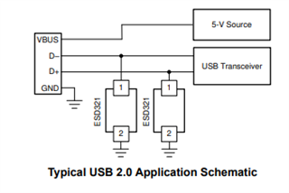
My design has 2 boards; a panel-board and main-board.  The main-board has an STM32F373 with a USB-C connector as well as ESD321DYAR diodes for DM and DP USB line protection.

The main-board can be used on its own, but can also be optionally connected into the panel-board ( a front panel ).  For convenience, I would like the panel-board to also have a USB C connector so that the user can plug a USB cable into the front panel instead of the main-board.  Both USB C connectors lead to the same USB virtual com port on the main board.

I would like to add ESD321 protection close to both connectors, but noticed having 2 ESD on the DM/DP lines instead of 1 ESD resulted in failed USB communication.  I'm assuming the 1.4V drop ( instead of 0.7V ) caused by the diodes is too much and causing the failed comm.  

What is the best way to ESD protect both connectors?  I currently only have ESD diodes close to the main board connector, but am concerned they are too far away from the panel-board connector to protect adequately.   Should I add jumpers to allow the user to disable the main board USB connector if/when the panel-board is used?

Thank you

  • Hi Lou,

    I'd be happy to help here, but first I would like to get some clarification on the layout of your design.

    Is there any circuitry between the ESD321 devices placed on the panel-board USB-C connector and the ESD321 devices on the main-board? If so, what are the part numbers of these devices?

    If there are no devices between the panel-board protection and the main-board protection, then I believe the main-board protection will be sufficient. If there are other devices, we will work through the best solution for protecting this system!

    Also, just to clarify, is the connection between the front panel and the main-board simply a USB-C cable, or are these boards connected physically (by via or similar means)?

    Please let me know if you have any questions!

    Best Regards,

    Josh Prushing

  • Great, thanks!

    There is no circuitry between the panel-board to the main-board for the USB traces, other than the STM32 at the end of the traces.  The intent is to have traces from the main-board USB to the panel-board act as a 'USB extension cable' in a way, but with PCB traces.  There could potentially be some components/circuits 'near' the USB traces leading from the front-panel to the main-board, but none are directly connected to that 'USB circuit'.  We could ensure our design has USB traces going from the front-panel to the USB connector on the main-board ( right to the ESD321s ) instead of leading to the STM32 pins.   The STM32 is the only component on the USB traces.

    Also, the panel-board and main-board are connected via I2C, as well as shared +12V power supply and GND.  The +12V power supply goes into a separate voltage regulator for each board.

    Thanks again for your help!!

  • Hi Lou,

    Thanks for the clarification here! The ESD321 devices on the main-board will be sufficient to protect the USB-C connector across both use cases.

    We could ensure our design has USB traces going from the front-panel to the USB connector on the main-board ( right to the ESD321s ) instead of leading to the STM32 pins. 

    Just to make sure, the ESD321s are in parallel to the D+ and D- lines, correct? An example is shown below:

    Understood on the connection between the boards, thanks for providing clarity here as well!

    Best Regards,

    Josh Prushing

  • Ok, great thanks.  

    I did have a second question, Is there a larger package than the 0403 that can be used for USB ESD protection?

    Thanks

  • Hi Lou,

    TI offers many different package sizes, but I am unsure of the best way to share these in a consolidated manner. The best option I can think is to take a look at our Product Selection Tool and filter the specifications you need, and review the various packages for the devices that meet your specifications. Please keep in mind that some of these packages are leadless (like 0201 and 0402), while others are leaded (like SOT23 and SOD323). 

    If you have any questions on which packages are leaded/leadless, you can look at the "Pin Configuration and Functions" section in the datasheet, or you can always feel free to ask here Slight smile

    Please let me know if there is anything else I can assist you with!

    Best Regards,

    Josh Prushing

  • Perhaps I should first ask for assistance on how to determine pin 1 from pin 2 ESD321DYAR since that is why i'm looking for a larger/different package to begin with.

    The datasheet shows pin 1 to IO and pin 2 to GND, but then shows a table stating pin 1 and pin 2 are swapped for DYA package which I am using.  To confirm, should I connect pin 1 to GND?  

    Also, I do not see any 'marking' on the part so unable to determine pin 1.  Is pin 1 on the left side of the '1L3' label?  

    Thanks for the info.

  • Hi Lou,

    I'm not sure why this device is the sole exception in our portfolio, but for the DYA package, pin 2 should be connected to IO and pin 1 should be connected to GND. There should be a small circular indent in the top left corner, which would designate pin 1. If you cannot locate this indent, I believe pin 1 would be on the "3" side of the label. 

    I hope this clarifies this pin layout, I apologize for the confusion here!

    Best Regards,

    Josh Prushing