This thread has been locked.

If you have a related question, please click the "Ask a related question" button in the top right corner. The newly created question will be automatically linked to this question.

DP83867E: DP83867E: Xilinx Zynq mpsoc SGMII mode with TI DP83867 PHY link issue

Part Number: DP83867E

Hi,

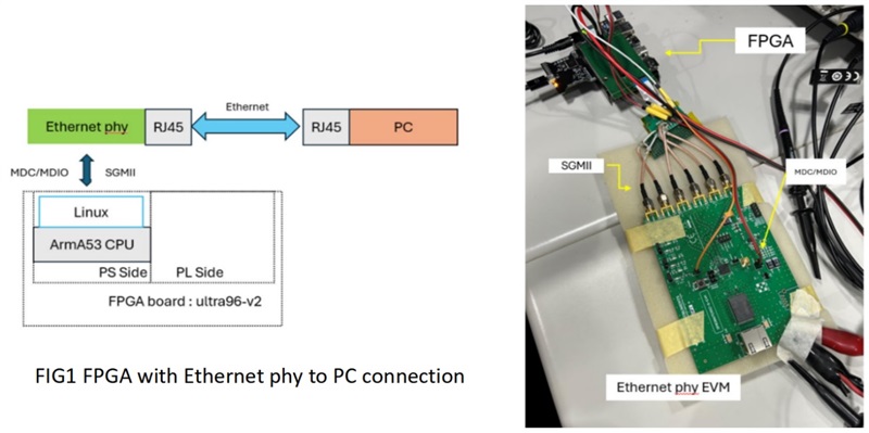
We have DP83867E SGMII EVM communicating with ultra96v2 by SGMII (6 wire),  We read registers by mdio interface, but it cannot ping PC. 

SGMII can no signal. 

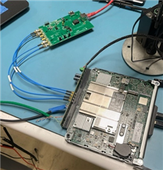
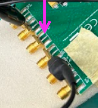
As Fig1. Current use ultra96v2 PS side A53 CPU with Linux and we want to use SGMII mode with TI DP83867E PHY (DP83867E EVM) connection.  


The following are confirmed: 

  1. Linux boot checking:
    FPGA FSBL loader can initial ethernet phy(ethernet@ff0b0000),macb drive link up to 100M

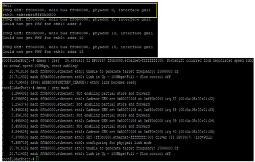
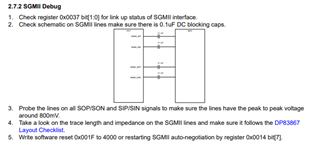
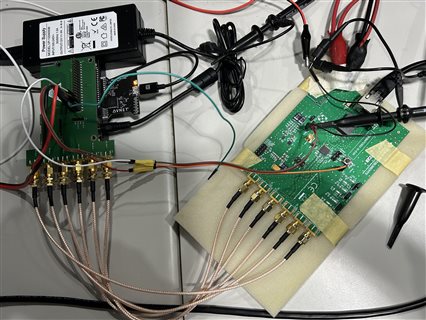
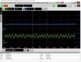
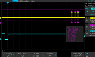
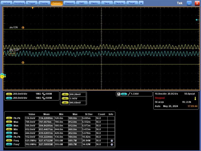
  2. Check MDIO/MDC and clk output waveform
    Yellow: MDC,Pink: MDIO, Green: DP83867E CLK output
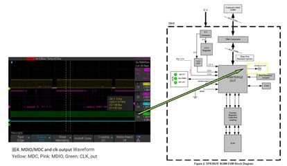
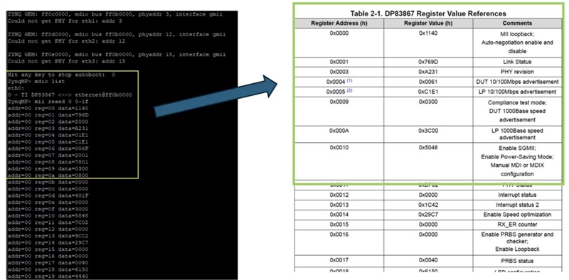
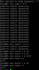
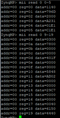
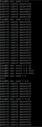
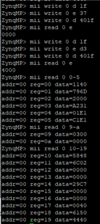
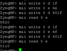
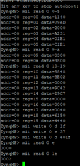
  3. uboot mii check
    here is mii read 0-1f. Some register status I don't know how to solve.

    a. BMSR bit2 alway 0 ,How can I solve?

    b. d3 set 4000 but read will be 0000. Why can i set SGMII 6 wire mode?
    c. CFG4(addr 31 ): 0002

  • Hi Tang,

    Thank you for sharing the information. Regarding to the SGMII debug, we have a new section on the DP83867 trouble shooting guide. Could you take a look on the following section?

    • Mainly looking for register 0x0037.

    Here is the document for the new revision of the trouble shooting guide:

    --

    Regards,

    Hillman Lin

  • Hi Hillman,

    Thank your reply.

    I recheck  phy init code in my bootloader as follow:

    hareware reset
    mii write 0 d3 4000
    mii write 0  0 1140
    mii write 0 16f 10M_SGMII_RATE_ADAPT = 0
    mii write 0 31  Set SGMII autonegotiation timer to 11ms
    mii write 0 32  0

    and I use uboot mii read 37 is 0000

    I use mii write reg 31 be 0x0060 after that I read reg 31 is 0000. 

  • Hi Chiehi,

    It seems like the main issue occur on the SGMII side. Based on your setup, it seems like your SGMII communication is not perfectly length matching with the EVM. I think the major issue lies on the connection between EVM <--> converter board <--> to the SoC. SGMII communication have a really strict standard on length matching. Based on the observation, we recommend to have better connection for SGMII communication.

    --

    Regards,

    Hillman Lin

  • Hi Hillman,

    I modify phy init code in my bootloader as follow:  (just remove mii write 0 d3 4000)

    hareware reset
    
    mii write 0  0 1140
    mii write 0 16f 10M_SGMII_RATE_ADAPT = 0
    mii write 0 31  Set SGMII autonegotiation timer to 11ms
    mii write 0 32  0

    And I get much better connect board. Can you suggest for SGMII legnth ?

    use mii read 0-5, 10-19,There is some different reg compare with snla246c, others are correct.

    reg = 04 data = 01E1  ;(default: 0061)

    reg = 0a data = 7800  ;(default: 3C00)

    reg = 11 data = be02  ;(default: BF02)

    reg = 19 data = 4440  ;(default: 4444)

    mii read 37 is 0000. And if I try to write d3 = 4000,then read reg 0-5,9-19 again, they will be incorrect value.

  • Hi Tang,

    Thank you for modifying the setup.

    Based on the picture, it seems like there are still multiple converters between SGMII communication. Could customer probe the SGMII signal near both end of the PHYs? We want to confirm on the signal waveform mainly looking for peak to peak voltage.

    --

    Regards,

    Hillman Lin

  • Hi Lin,

    Tnank your reply.

    I correct FPGA SGMII  pinout and I recover phy init code in my bootloader as follow:  (just add mii write 0 d3 4000)

    Is it complete for 6-wire SGMII initial  in my phy init code? Or can you provide a sample code for 6-wire phy initial ?

    hareware reset
    mii write 0 d3 4000
    mii write 0  0 1140
    mii write 0 16f 10M_SGMII_RATE_ADAPT = 0
    mii write 0 31  1071  (Set SGMII autoneg timer to 11ms)
    mii write 0 32  0

    For connection I find this reference as follow fig . So I think my cable should be ok.


    For now d3 register value can be 4000,and others register are normal. but 0x37 still zero As follow.

    And all of SGMII pin(SI/CO/SO) still no signal. But some of they have 1~1.5v.  


    If I set register d3 to 4000 successfully. DP83867 will generate clock(COP/CON) to FPGA ,right?  or  it need other conditions meet ?

  • Hi Tang,

    I will review it and provide you an response later.

    --

    Regards,

    Hillman Lin

  • Hi Tang,

    Just wondering when you measure the SGMII Vpeak to peak.

    Are you measuring from the SOP an SON pin? or SIN and SIP pin? We are expecting around 2.2V SGMII output. 

    If possible, could you provide a eye diagram scope capture on SOP/SON or SIN/SIP?

    --

    Thank you,

    Hillman Lin

  • Hi Lin,

    Thanks your reply.

    I use 20GSa/s scope capture on SOP/SON as fig ,it's 500mv for V peak to peak.

    We check delay to 200ms for spec today. But it still ping unable. 

    Are there some sgmii signals can check after reset ?  

  • Hello,

    Hillman is OoO and will be responding tomorrow.

    Sincerely,

    Gerome

  • Hi Tang,

    500mV Vpp seems small to me. I see alot of reflection on the SGMII signal. May I ask where is the probing position?

    May I ask what is the second figure scope capture? Is it MDIO/MDC and reset lines?

    --

    Regards,

    Hillman Lin

  • Hi Lin,

    We recheck FPGA pinout.There is 1.8v output for mdc/mdio.

    And DP83867 use 2.5 vdd ,so we will try external 1.8v supply first.  

    After that we will feedback resullt.

  • Hi Tang,

    I will wait for your feedback.

    --

    Regards,

    Hillman Lin

  • Hi Lin,

    We use FPGA(ultra96v2)for 1.8v and  power supply 5v.

    initial reg as follow, 0x37 still 0, 

    The sgmii still no signal.If I probe fpga sma connector as follow fig (sgmii disconnect and mdc/mdio connect).

    fpga sgmii pin voltage as follow (pk-pk only 40mv)

    SIN 1.2v

    SIP 0

    CON 700mV

    COP 500mV

    SON 700mV

    SOP 500mV


  • Hi Tang,

    It seems like SIN and SIP DC offset does not seems right to me. 

    DP83867PHY should output around 1V Vpp. Not sure what is degrading the signal. If possible, could you try changing the link partner to anther DP83867EVM and see if you see the similar observation? We want to check is SOP and SON connection are good.

    --

    Thank you,

    Hillman Lin

  • Hi Lin,

    recheck VDD and connection

    The phy clk as follow

    There is 1.2v externl from FPGA and it would let phy so offset 1v. Is it correct for SGMII sgmii signal for phy SO to FPGA?

    phy SO disconnect with MAC phy SO connect with MAC
      phy SO disconnect with MAC     phy SO connect with MAC


    There is phy SI signal. 

  • Hi Chiehi,

    I am not sure if my understanding is wrong for your measurement. PHY clock (XI pin) should be 25MHz instead of 625MHz. 

    Regarding to the SGMII measurement, the waveform is not too clean. May I ask where did you probe this measurement? Which position did you probe it?

    When you did not connected to MAC for SGMII measurement, did you have 100 ohms termination while you are probing the measurement?

    --

    Regards,

    Hillman Lin