This thread has been locked.

If you have a related question, please click the "Ask a related question" button in the top right corner. The newly created question will be automatically linked to this question.

SN65DSI86-Q1: DP link training fails

Part Number: SN65DSI86-Q1
Other Parts Discussed in Thread: SN65DSI86, TEST2

Tool/software:

Hi Ti teams,

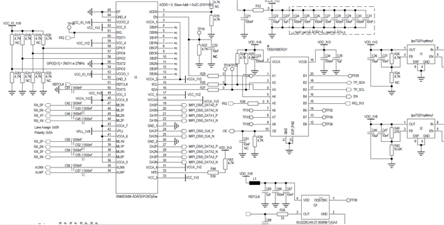
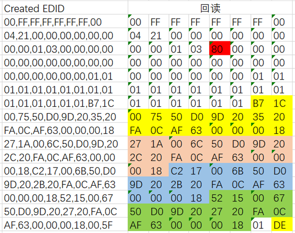
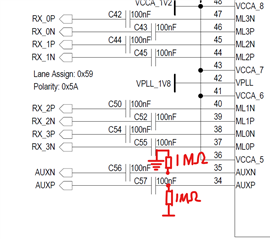
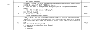
We use SN65DSI86 to display color bar pattern,but only black display. The value of register 0x96 is 0x00, and the value of register 0xF8 is 0x12. The link training is fail.

The number of DP lanes we used is 4, and the DP data rate is 1.62Gbps. 

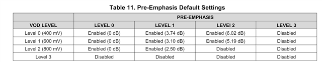
We want to change the Link Training Look-Up-Table default value, could you give me same advice  what is the appropriate value. 

Best Regards

Emily

  • Emily

    Table 11 in the DSI86-Q1 datasheet lists the pre-emphasis default setting, 

    You can modify the values in the DP Link Training Lookup Table, but the default values should pass link training in most cases. If needs to be changed, the default values have to be depend on your eDP/DP signal measurement result. 

    Can you please share your schematic, eDP/DP resolution EDID, and DSI86-Q1 register programming values?

    Thanks

    David

  • Hi David,

    The FPC we used between SN65DSI86 and display is single layer, and not differential wiring. Is this the cause for the link training failure?

    The schematic, eDP/DP resolution EDID, and DSI86-Q1 register programming values are showing as below.

    We pull TEST2 pin to 1.8V thru a 4.7k resistor.

    add = 0x0A;//ref clk 27M hz
    regmap_write(pdata->regmap, add,0x06);
    regmap_read(pdata->regmap, add, &read_val);
    DRM_ERROR("IIC read back add %x val %x\n", add,read_val);

    add = 0x5C;// disable hdp
    regmap_write(pdata->regmap, add,0x00);
    DRM_ERROR("IIC set add %x val 00\n", add);
    regmap_read(pdata->regmap, add, &read_val);
    DRM_ERROR("IIC read back add %x val %x\n", add,read_val);

    add = 0xE9;// enable fail int
    regmap_write(pdata->regmap, add,0xFF);
    regmap_read(pdata->regmap, add, &read_val);
    DRM_ERROR("IIC read back add %x val %x\n", add,read_val);

    add = 0x10; // 4 dsi lanes
    regmap_write(pdata->regmap, add,0x26);
    regmap_read(pdata->regmap, add, &read_val);
    DRM_ERROR("IIC read back add %x val %x\n", add,read_val);

    add = 0x12; // dsi clock =freq 221Mhz
    regmap_write(pdata->regmap, add,0x2C);
    regmap_read(pdata->regmap, add, &read_val);
    DRM_ERROR("IIC read back add %x val %x\n", add,read_val);


    add = 0x59; //aling is 3210
    regmap_write(pdata->regmap, add,0x1B);
    regmap_read(pdata->regmap, add, &read_val);
    DRM_ERROR("IIC read back add %x val %x\n", add,read_val);

    regmap_write(pdata->regmap, 0xff,0x07);
    regmap_write(pdata->regmap, 0x16,0x01);
    regmap_write(pdata->regmap, 0xff,0x00);
    add = 0x5A; //f4 polor enhanced framing and assr
    regmap_write(pdata->regmap, add,0xF4);
    regmap_read(pdata->regmap, add, &read_val);
    DRM_ERROR("IIC read back add %x val %x\n", add,read_val);

    add = 0x93; //4 dp lanes no scc
    regmap_write(pdata->regmap, add,0x34);
    regmap_read(pdata->regmap, add, &read_val);
    DRM_ERROR("IIC read back add %x val %x\n", add,read_val);

    add = 0x94; //hbr 1.62G bps
    regmap_write(pdata->regmap, add,0x20);
    regmap_read(pdata->regmap, add, &read_val);
    DRM_ERROR("IIC read back add %x val %x\n", add,read_val);

    add = 0x0d; //pll enable
    regmap_write(pdata->regmap, add,0x01);
    msleep(10);
    regmap_read(pdata->regmap, add, &read_val);
    DRM_ERROR("IIC read back add %x val %x\n", add,read_val);
    msleep(10);

    add = 0x0A; // training mode should 0x01
    regmap_read(pdata->regmap, add, &read_val);
    DRM_ERROR("IIC read back add %x val %x\n", add,read_val);

    add = 0x95; //
    regmap_write(pdata->regmap, add,0x00);
    regmap_read(pdata->regmap, add, &read_val);
    DRM_ERROR("IIC read back add %x val %x\n", add,read_val);

    add = 0x96; // auto training
    regmap_write(pdata->regmap, add,0x02);
    msleep(5);
    regmap_write(pdata->regmap, add,0x0A);
    msleep(200);
    regmap_read(pdata->regmap, add, &read_val);
    DRM_ERROR("IIC read back add %x val %x\n", add,read_val);
    msleep(10);

    /* config video parameters */
    ti_sn_bridge_set_video_timings(pdata);

    add = 0x5B; // 24bpp
    regmap_write(pdata->regmap, add,0x00);
    regmap_read(pdata->regmap, add, &read_val);
    DRM_ERROR("IIC read back add %x val %x\n", add,read_val);

    add = 0x3C; // color bar
    regmap_write(pdata->regmap, add,0x10);
    regmap_read(pdata->regmap, add, &read_val);
    DRM_ERROR("IIC read back add %x val %x\n", add,read_val);

    msleep(10);
    add = 0x96; // training mode should 0x01
    regmap_read(pdata->regmap, add, &read_val);
    DRM_ERROR("IIC read back add %x val %x\n", add,read_val);

    add = 0x5A; // en
    regmap_write(pdata->regmap, add,0xFC);
    regmap_read(pdata->regmap, add, &read_val);
    DRM_ERROR("IIC read back add %x val %x\n", add,read_val);

    msleep(10);

  • Hi,

    Have you used DSI86 spreadsheet to calculate its register programming value? For DSI86 configuration, use the spreadsheet in this e2e post, https://e2e.ti.com/support/interface-group/interface/f/interface-forum/945404/faq-sn65dsi86-how-do-i-programming-the-sn65dsi86-registers

    Looking at the EDID, it seems the vertical front porch value (EDID Register Address 0x40 and 0x41) are too large for the DSI86 register space which means the DSI86 may not able to support this particular panel. 

    I attached color bar with and without ASSR examples, can you see if either one of them works?

    3513.2DP_4DSI_RBR_800x600_Color_Bar.zip

    2DP_4DSI_RBR_800x600_Color_Bar_ASSR.zip

    Thanks

    David

  • Hi David,

    Yes,we have used DSI86 spreadsheet to calculate its register programming value.

    The table below is the eDP/DP panel timing we get from panel EDID.  

    73,51 DCLK
    1280 H Active
    117 H Blanking
    720 V Active
    157 V Blanking
    53 H front porch
    32 H Sync Width
    32 H back porch
    63 V front porch
    10 V Sync Width
    84 V back porch

    The SN65DSI86 Register settings are same as EDID.

    [ 6.233856] [drm:ti_sn_bridge_enable] *ERROR* IIC read back add 20 val 0
    [ 6.234316] [drm:ti_sn_bridge_enable] *ERROR* IIC read back add 21 val 5
    [ 6.234334] [drm:ti_sn_bridge_enable] *ERROR* sean bridge set video hdisplay 1280
    [ 6.237625] [drm:ti_sn_bridge_enable] *ERROR* IIC read back add 24 val d0
    [ 6.238119] [drm:ti_sn_bridge_enable] *ERROR* IIC read back add 25 val 2
    [ 6.238141] [drm:ti_sn_bridge_enable] *ERROR* sean bridge set video vdisplay 720
    [ 6.238906] [drm:ti_sn_bridge_enable] *ERROR* IIC read back add 2c val 20
    [ 6.238924] [drm:ti_sn_bridge_enable] *ERROR* sean bridge set video end-start 32
    [ 6.239681] [drm:ti_sn_bridge_enable] *ERROR* IIC read back add 2d val 80
    [ 6.239701] [drm:ti_sn_bridge_enable] *ERROR* sean bridge set video hsync_polarity 128
    [ 6.240460] [drm:ti_sn_bridge_enable] *ERROR* IIC read back add 30 val a
    [ 6.240481] [drm:ti_sn_bridge_enable] *ERROR* sean bridge set video vsync end - start 10
    [ 6.242613] [drm:ti_sn_bridge_enable] *ERROR* IIC read back add 31 val 80
    [ 6.242641] [drm:ti_sn_bridge_enable] *ERROR* sean bridge set video vsync_polarity 128
    [ 6.243402] [drm:ti_sn_bridge_enable] *ERROR* IIC read back add 34 val 20
    [ 6.243419] [drm:ti_sn_bridge_enable] *ERROR* sean bridge set video htotal - end 32
    [ 6.244174] [drm:ti_sn_bridge_enable] *ERROR* IIC read back add 36 val 54
    [ 6.244193] [drm:ti_sn_bridge_enable] *ERROR* sean bridge set video vtotal - end 84
    [ 6.245838] [drm:ti_sn_bridge_enable] *ERROR* IIC read back add 38 val 35
    [ 6.245863] [drm:ti_sn_bridge_enable] *ERROR* sean bridge set video hstart - hdisplay 53
    [ 6.247003] [drm:ti_sn_bridge_enable] *ERROR* IIC read back add 3a val 3f
    [ 6.247023] [drm:ti_sn_bridge_enable] *ERROR* sean bridge set video vstart - vdisplay 63

    Best Regards

    Emily

  • Hi David,

    For DP display,we pull TEST2 pin to 1.8V thru a 4.7k resistor, and add a 1MΩ resister on AUX_P and 1MΩ resister on AUX_N.The HPD is option, and the function need to be disabled. Is it correct?

    For eDP display, the TEST2 pin is connected to the ground, and no pull-up resister on AUX_P and no pull-down resister on AUX_N.The HPD is necessary.Is it correct?

  • Hi,

    The HPD I/O cell has an internal 60-kΩ pull-down resistor. The HPD pin requires a series external 51-kΩ 1% resistor as depicted in Figure 6. According to the VESA Embedded DisplayPort standard, use of HPD is optional for a DisplayPort transmitter. If the system designer chooses to not use HPD, then software must disable HPD by setting the HPD_DISABLE bit.

    For DP AUX, you would need to have 100k pulldown to ground on AUXP and 100k pullup to DP_PWR on AUXN. 

    DP does not support ASSR, so you would pull TEST2 pin to 1.8V through a 10k resistor, and use Standard DP Scrambler Seed in register 0x5A

    For eDP, pullup/pulldown on AUX is optional and depends on the eDP sink requirement. If eDP supports ASSR, then use Alternative Scrambler Seed Reset 

    Are you able to program the DSI86 with the two examples I gave and see if they work?

    Thanks

    David

  • Hi David,

    For DP panel, the display supplier recommends us to add a 1MΩ pull-up resister on AUX_P and 1MΩ pull-down resister on AUX_N,which is conflict with the requirement from TI.The AUX communication is successful, but the link training is fail. We don't know why the link training is fail.

    When change the panel configuration to eDP interface,and keep the TEST2 connected to GND, and no pull up and pull down resister on AUX channel, the link training is successful.There is no display because the eDP panel can't support ASSR. We are waiting for the new configuration panel which can support ASSR from supplier.

    I didn't try the example you sent to me, because some register settings are different with our design.For example,the lane configuration and polarity need to be changed.

  • Hi,

    Most DP monitors do not support ASSR. If this is the case, DSI86’s ASSR will need to be disabled by making ASSR_CONTROL read/write instead of read-only. The first step to make ASSR_CONTROL read/write is to make sure TEST2 pin is be sampled high at the rising edge of EN pin. It is recommended to pull TEST2 pin to 1.8V thru a 1k to 10k resistor. Once TEST2 is high, the following steps must be performed:

    1. Write 0x07 to register 0xFF. This will select Page 7.
    2. Write 0x01 to register 0x16. This will make ASSR_CONTROL to be read/write.
    3. Write 0x00 to register 0xFF. This will select Page 0.
    4. Write 0 to bits 1:0 at register 0x5A. This will change from ASSR to Standard DP.

    Have you done step 1 through 4?

    Thanks

    David

  • Hi David,

    Yes, the TEST2 has been pulled up to 1.8V through a 4.7kΩ resistor, and the registers have been configured as blow, but the DP training is fail.

    regmap_write(pdata->regmap, 0xff,0x07);
    regmap_write(pdata->regmap, 0x16,0x01);
    regmap_write(pdata->regmap, 0xff,0x00);
    add = 0x5A; //f4 polor enhanced framing and assr
    regmap_write(pdata->regmap, add,0xF4);

    Best Regards

    Emily

  • Emily

    After power up the DSI86-Q1, and you write 0xFF to register 0xF8 to clear it, can you please read register 0xF8 after the link training failed to see which error has been reported?

    Is it possible to change the FPC you used from single layer to differential wiring?

    Thanks

    David

  • Hi David,

    When DP link training is fail, the value of 0xF8 is 0x12. When we change the FPC from single layer to differential wiring, the DP link training is still fail.We didn‘t find the root cause.

    We got eDP panel that can support ASSR from supplier today, now it works.

  • Emily

    For the non-ASSR panel, if you write 0x0010 = TPS1 to register 0x96 first, then 0x1010 = Semi-Auto Link Training, does this resolve the link training? Or are we considering the issue to be closed since link training is working now with the ASSR panel?

    Thanks

    David