SN65HVD01: SN65HVD01 Power Consumption

Part Number: SN65HVD01
Other Parts Discussed in Thread: SN65HVD10

Tool/software:

Team, 

About the SN65HVD01, I checked the datasheet and have one question about the power consumption of this component.

In my customer design, the signal rate is very low (1pps) or data/ctrl message (<500kHz).

  1. We want to know what’s the typical and maximum power consumption of SN65HVD01 when it’s supplied by 3.3V.
  2. When SN65HVD01 is in driver or receiver mode, does the typical/maximum power consumption is same? If not, what’s the value for driver or receiver?

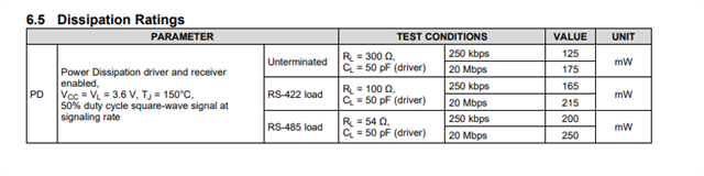
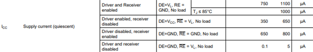
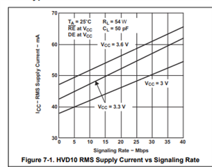
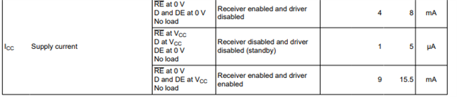
And we also got same question about the SN65HVD10, can you also share the data?

Thanks!

Regards,

Qiang

  • Hi Qiang,

    Our expert is currently out of office, he will respond here after his coming backing tomorrow.

    Regards,

    Sean

  • Hi Qiang,

    Before I get into your power question - how precise does the 1pps signal need to be - I am asking because RS-485 is generally not a good device choice for 1pps signals, not because data rate but because a lot of these types of signals require a very high level of precision that you won't get from RS-485 and if the pulse width is small enough RS-485 may not be fast enough to work. 

    So please if you could confirm:

    1. What level of pulse skew is acceptable 

    2. What is the pulse width of the signal 

    With that being said a few things:

    For your first Question:

    Power consumption can be thought in terms of current into VCC and VL pins - we will all the current usage ICC_total for simplicity. ICC_total = ICC(q) + I_Load + I_AC_LOSS where power consumption is just ICC_total * VCC. ICC(q) is the quiescent current and is listed in the datasheet. I_Load is dependent on system setup - in RX mode it is the current sourced from the "R" pin and in TX mode its the current sourced from differential driver. I_AC_LOSS is not spec'd directly but indirectly through power dissipation table for this device. 

    The frequency is 1Hz essentially so you are really going to be looking at more of a DC power usage - which means we can ignore most AC losses and just focus on DC losses (this isn't strictly true - but its the best estimate you are going to get from datasheet)


    If you look at the power dissipation rating - the worst case you should be looking at is probably the 250kbps rating - which is ranges from 125mW to 200mW depending on loading (RS-485 loading worst case). The 250kbps is probably the closest you can estimate - but customer will have to test in system to get their max for their use case - but most likely it would be <= 200mW. This includes ICC(q), I_AC_LOSS, and I_LOAD (for driver side, receiver side assumed low current). There will be loss for short 1pps pulse widths but over the period of 1 second it will be averaged out to around the 250kbps level if not lower. 

    For your second question


    In general the driver current is going to be more than the receiver current if they are both loaded as generally the current for the RS-485 bus is typically around 60mA compared to much lower on the "R" output (depends if there is a bias resistor or not - if not generally you are looking at uA level currents a lot of the time - but up to +/-8mA is pretty standard though) 

    But the ICC(q) (no load ICC current) is going to be higher for RX enabled and TX disabled for this device - however when load currents are considered the power is going to be higher on the driver - if unloaded it will the be the receiver. 

    For the HVD10 device - we don't have a power dissipation table (we have a max rating - but that is different than the actual consumption of the device) - but we do have a typical plot that gives the typical power consumption for an RS-485 load - this includes ICC(q), Load current, and AC loss current.  It only includes a load between A and B however. This is the best approximation. 

    The receiver is similar on this device in that it consumes more power when there is no load

    but when loaded the driver section is going to consume more power because the output drive current is larger than Receiver output current. 

    However similar questions on the PPS signal requirements because the vast majority of PPS applications are not suited for RS-485 due to a high amount of precision common to PPS signal applications  (there are exceptions - which is why I want to know the pulse width and skew requirements of the PPS signal in this system because it may work)

    Best,

    Parker Dodson

  • Parker,

    Thank you so much for your detailed explanation on the power consumption.

    About the signal spec question:  For 1pps, they care more about rise time, delta of delay time. And in my customer Mass Production project, they are using the SN65HVD10 for 1pps and works well.

    And one more application risk to check is: When we are using RS485 device 0 work as transmitter in board A, work as driver mode(DE mode), use RS485 device 1 work as receiver in board B. But board B is powered off. Is there any risk of this application, like the latch off? Transmitter working in DE mode, receiver powered off. 

    Thanks

    Regards,

    Qiang

  • Hi Qiang,

    I am glad that my explanation was helpful. 

    That is good to hear on the PPS signal - if they already have had good results with the device with 1pps than I withdraw my concern. There are applications that use 1pps that RS-485 can work for - but some pps applications require very high precision. I am glad that this application works well with RS-485 devices. 

    For your other question

    Board A - Transmitter with DE = 1 and Board B with a receiver that is powered off - is there risk here?

    The answer is generally no risk as long as the voltage between A and B remains between the abs max ratings listed in the datasheet

    So as long as unpowered receiver sees a voltage between -13V and 16.5V on the A  pin (w.r.t. GND) and the B pin (w.r.t. GND) there shouldn't be an issue. 

    The receiver input voltage range is independent of VCC - if it wasn't you would see "VCC + Vd" (where Vd is some forward voltage for an ESD diode) listed as the max. Since it is just an absolute voltage range - it is independent of VCC level - so VCC = 0V the range will remain the same.  

    The unpowered device must be grounded or else the pin will not have a stable reference and you could see issues. 

    The only risk (which is extremely unlikely - as this risk would cause the application to fail even when both devices are active most likely - so it is extremely unlikely to be an issue) - is that if there is a large ground potential difference - i.e. the voltage drop between the GND on board A and the GND on board B is large enough that the the voltage received + Ground Potential Difference >= abs max limit - there could be a problem. However, this risk is minimal because that would be a problem regardless of VCC state and the ground potential difference would need to be very large (larger than most RS-485 applications would expect).

    Please let me know if you have any other questions and I will see what I can do. 

    Best,

    Parker Dodson