SN65LBC173A-EP: SN65LBC173A-EP/SN65LBC174A-EP Receiver and transmitter end Circuit configuration.

Part Number: SN65LBC173A-EP
Other Parts Discussed in Thread: SN65LBC174A-EP, SN65C1167E

Tool/software:

Hi,

This question is a continuation of the one in the link below.

e2e.ti.com/.../sn65c1167e-alternative-to-sn65c1167e-for-higher-ambient-temperature

Based on the suggested list of Transceivers, I have chosen SN65LBC173A-EP as a receiver and SN65LBC174A-EP as a transmitter. The application is to send the PWM signals (100kHz) from the control board to the gate driver board differentially, whose duty will vary from 5% to 95% (pulse width of 500ns to 9.5us), and the dead time would be between 100ns to 300ns between the PWM’s driving Top and Bottom switch. The distance to be sent would be around 150cm to 200cm.

 I plan to use the receiving end circuit, as shown below (Figure 1). The 549-ohm resistors are a failsafe resistor. And 10 ohms series resistors are used from a design guide, “Protecting RS-485 Interfaces Against Lethal Electrical Transients”. I intend to use the TVS diode Between (R7 & R8) and C2.

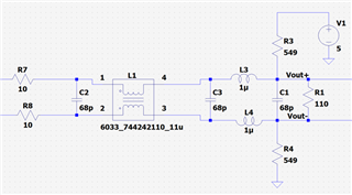
Figure 1: Receiver end circuit

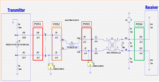
This circuit is similar to the one used in the UCC217XXQDWEVM-054 but has an additional common mode choke with capacitors (Figure 1). The transmitter side circuit is not present in the UCC217XXQDWEVM-054. The signal to be sent goes to the transceiver input channel, and the output differential signal is directly routed to a connector.

1) Is there any suggestion for a transmitter side circuit for the SN65LBC174A-EP?

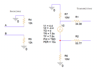
2) As there is no LTspice model for SN65LBC174A-EP, I tried an LTspice simulation with SN65C1167E (as given in the UCC217XXQDWEVM-054). I am aware of the fact that SN65C1167E is an RS422. However, since the models for SN65LBC173A-EP and SN65LBC174A-EP are not available, I went with this option. The model was tried with NO transmitter end circuit (as shown in Figure 2) while using the cable impedance of 120 ohms and Td=50ns.

Figure 2: Simulated Circuit

The simulated circuit gave the below outputs.

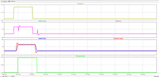
Figure 3: Simulated Circuit (Figure 2) output waveform

Even though the output signal looks fine, there is significant distortion in the transmitted signal. Do you suggest any transmitter side circuit to mitigate these distortions? Any general comments?

3) I have modified the circuit on the transmitter side as shown below (Figure 4) (i.e., adding an LC filter on the transmitter side).

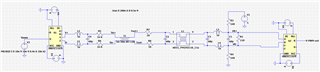
Figure 4: Modified Simulated Circuit

The output waveforms of the modified circuit are shown in Figure 5. The distortion seems to be a bit better on the transmission side; however, the overall distortion in the transmission and receiving signals is unsatisfactory. Please let me know how to improve the transmission and receiver side circuit to get proper transmission and receiving end signals.

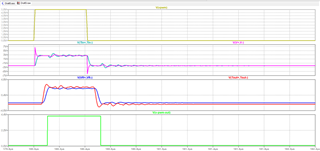
Figure 5: Modified Simulated Circuit (Figure 4) waveform

Additional Information: I have used 549 ohms for fail-safe biasing. So the overall Receiving side impedance will be 110||(2*549) = 99.98 ohms. If we consider series 10 ohms resistors as a part of the load, I thought the overall impedance at the receiving end would be 120 ohms, and hence, I used the cable impedance to be 120 ohms. Is this assumption right?

4) Could you please recommend a TVS diode that could be used for SN65LBC173A-EP and SN65LBC173A-EP. According to the datasheet, diodes need to be bi-directional, and they cannot clamp below -10V or above 15V - and you shouldn't conduct at 6V or less - so the voltage rating needs to be 6V or higher but the max clamped value needs to be in-between -10V to 15V. I am unable to find such TVS diodes that can clamp at -10V and +15V.

Thank you

  • Hi Vijaymahantesh,


    - Make sure you have a termination resistor on the transmitter end as well. Then you can just connect the transmitter differential lines to the bus.  

    - We do not support LTspice modeling unfortunately. I would recommend not using the RS-422 part as it has different behavioral characteristics.

    Instead, below is a bus facing model that should be relatively accurate for quick measurements. The PW will be determined by your desired duty cycle.


    - What kind of surge are you anticipating the system to encounter? Additionally, how long is the surge length you are expecting?

    Best,

    Ethan

  • 1) For unidirectional signals, you do not need a termination resistor at the transmitter. In general, you would add the same protection components at both transmitter and receiver; what components to use depends on what kind of transients you expect. (Most of your components remove high frequencies; the common-mode choke can also remove common-mode noise at the same frequencies as your signal.)

    2) The differential signal at the receiver (VR+ − VR−) looks OK.

    3) Too many capacitors and inductors might introduce ringing at some resonant frequency. Consider using fewer components.

    The termination's total impedance should match the cable impedance.

    4) RS-4xx receivers accept a wide common-mode range, but your TVS diodes need to handle only the signal voltages that actually happen on your bus. Can there be an offset between both grounds? When both nodes use the same ground, then your actual signals will be somewhere between 0 V and 5 V.

  • Vijaymahantesh,

    All of Clemens points are accurate. Please give us all information possible, and we can get back to you.

    Best,

    Ethan

  • Clemens,

    I am sorry for the delay in getting back to you. I am trying the simulation with the transmitter and receiver side equivalent circuit shown by 

    1) You said, "same protection components at both transmitter and receiver", If I understand it correctly, you mean to say that generally whatever the circuit present at receiver side is what is put on the transmitter side, that means Commom mode choke, capacitors, inductors and TVS diodes, except the termination resistors at the transmitter side (due to unidirectional). Am I right in interpreting what you said?

    or is it that only the protection circuit like 10 ohms and TVS diodes will be present both on the transmitter and receiver, however the CM choke and Inductor and capacitor will be only present on receiver side?.

    2)  I am trying the simulation with the transmitter and receiver side equivalent circuit shown by . I will reply soon with results.

    3) Okay I will try with fewer components.

    4) At this point in the development stage, I am not sure how to answer the question of "Can there be an offset between both grounds?". But I will be connecting two grounds (short both the grounds on the control board and gate driver board). And a 100 ohm from each ground to earth.

    on my point regarding equivalent impedance seen at the receiver, is it correct? (If we don't have any CM choke and Inductors and capacitors), is the below statement correct?

    I have used 549 ohms for fail-safe biasing. So the overall Receiving side impedance will be 110||(2*549) = 99.98 ohms. If we consider series 10 ohms resistors as a part of the load, I thought the overall impedance at the receiving end would be 120 ohms? 

    or do the series resistors 10 ohms cannot be taken as a part of load and cannot be added to 100 ohms. So, if so, do I need to make the fail-safe biasing resistors and termination resistors such that without 10 ohms, the equivalent impedance is 120 ohms ?

    Thank you

  • ,

    Thank you for the equivalent circuit. I will try it and get back. 

    At this point, I am very new to RS485 and I am not sure what kind of surge is expected, but the system is like this: the PWM signals will go from the control board to the gate driver board, the distance of which may be around 200cm. Overall, the hardware will be enclosed in some frame. Many isolated converters are used to get the voltages required for the Control board and gate driver board. With this, I don't expect any (ideally) transients whatsoever on the RS485 lines. But whatever I read of RS485, it has TVS diodes for the transients; I am not sure if TVS diodes need to be used only if you have very long-distance communication. Can you let me know if you have any experience with a short-length communication (around 200 cm) enclosed in some kind of aluminum frame if TVS diode protection is required?

    Thank you

  • Clemens, I have done a few simulations and am attaching the results (in pdf attached below). Do you have any comments on the configuration that you would recommend out of the simulated ones in PDF (attached below)? Or do you have any other suggestions which I should probably try out?

    I have one more question regarding the position of the 10-ohm pulse-proof resistors. As, in the figure below the 10-ohm pulse-proof resistors should be in POS1 and POS4 or POS2 and POS3?

    Transmitter_Receiver_CKT_simulation.pdf

    Thank you

  • Thanks for getting back to me, and I appreciate the clarification on your system. 

    A TVS diode is not required by the RS-485 standard, and adding that diode is to help with large transients (maybe induced by other wires/circuits in proximity). A longer bus length just signifies more opportunity for transients to occur, and it doesn't directly imply transient protection is necessary. Just to be safe, you can add TVS diode pads and decide to populate them with diodes later on. 


    In your simulation PDF, you do not need to worry about the noise on the V(Tin+/-) or the V(Tout+/-). The V R+/- is only what matters as it is what the receiver actually sees (by design the differential system is mitigating most of the noise). Even with the distortion on the VR line, it is still well within the threshold to determine high/low values on the receiver.  


    I would recommend Configuration - 1 with the POS1 and POS4 to have 10 Ohm pulse proof resistors. You should not have to worry about perfect impedance matching with these resistors as your bus length is shorter.


    Another note about your simulation, the transmission line Td value is not 50ns, it should be smaller. You can calculate the value with the signal propagation of your cable/trace and the cable length (in your case 200cm). Otherwise the simulation looks ok. 


    Let me know if you have any other questions, and if not feel free to mark as resolved. 

    -Ethan

  • ,

    Thank you for your recommendations. I have a couple more questions.

    1) I could not get the 556 ohms and 135 ohms resistors (fail-safe biasing and termination resistors). Instead, 549 and 133 ohms resistors of 0.5 watts (0805 package) are available, so do you think it is okay to go ahead with 549 and 133, with which we would get the termination resistor of around 118.6 ohms. 

    We are actually going to make a flexible PCB for connecting a control board to Gate drive board which will carry PWM differential signals. So with this arrangement if we make a differential routing signal impedance to be around 120 ohms is that okay?

    2) IS SM712 okay to use as a TVS diode for the SN65LBC173A-EP/SN65LBC174A-EP pair?

    Thank you

  • Vijaymahantesh,

    Those new resistor values you mentioned will be just fine. And 120 Ohms signal impedance is good. 

    Yes, the SM712 is okay to use for both devices. However, the ESDS552 might be cheaper depending on your configuration.

    -Ethan

  • Thank you for the reply. 

    I have one last question; it is regarding SN65LBC179QDR. I am using this (SN65LBC179QDR) IC to differentially send the Fault signal and receive the Reset signal. I.e fault signal from all the 4 gate drivers are combined using a logic circuit and given to SN65LBC179QDR for differentially sending it to control board. As SN65LBC179QDR has a receiver, it will receive the Reset signal from the microcontroller to be given to all 4 gate drivers. 

    So,

    1) As SN65LBC179QDR is a RS485. If I use the same transmitting side and receiving side circuit as discussed above for this (SN65LBC179QDR) IC, it should be oKay?, (i.e. Fail-safe biasing resistors and CM choke and LC filter and ESD diodes and 10-ohm pulse proof resistors).

    Thank you

  • Vijaymahantesh,


    From what I understand from your post, it should be okay assuming you follow the same practices mentioned throughout this thread. I cannot speak specifically to the data layer as RS-485 is only on the physical layer level. Overall, it may not be the most efficient methodology, but to me it certainly should work still. 


    Best,

    Ethan