A related question is a question created from another question. When the related question is created, it will be automatically linked to the original question.
If you have a related question, please click the "Ask a related question" button in the top right corner. The newly created question will be automatically linked to this question.
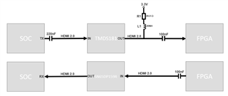
The termination network used to AC couple the HDMI outputs of the TMDS181 will result in an output swing that is cut in half. I recommend using the TDP0604 rather than the TMDS181 as the TDP0604 can receive DC coupled HDMI and internally bias for AC coupled HDMI output. This will improve signal integrity.
Are you able to swap the chip? Do you need a retimer in this application, or will a redriver suffice?
It seems AC coupling is required for the FPGA, so why is there no AC coupling for the DP159?
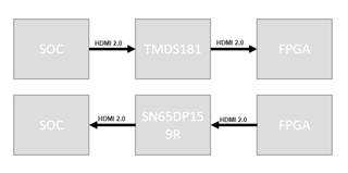
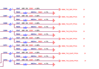
FPGA's GT transmitter/reciever does not support TMDS Level Signaling and need to use a re-timer to be compliant with TMDS specifications. So, I pick SN65DP159 and TMDS181 by following FPGA board design guide's recommendation.
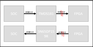
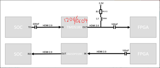
Please kindly see the diagram updated below. BTW, I am not sure if R1 and L1 and 100nF is needed at TMDS181 output side. I just refer to the FPGA reference SCH.
Will need pull up to 3.3V for valid DC coupled HDMI detection. After pullup AC cap will be required to AC couple signal. This will effectively cut the output signal swing in half. You will need to maximize swing from the SOC to compensate fro this. Another option is to use the TDP0604(6Gbps) or TDP1204(12Gbps) that can take and AC coupled signal and output an AC coupled output signal. This removes the need to external biasing on the HDMI lines.
Does SDA and SCL not go to the SoC? What is U17E
Additionally for U4005:
Is it ok to have DC coupled HDMI going to RK3588 SoC?
For U4005 make sure that the SOC is able to handle DC coupled HDMI. If the SOC is not able to handle DC coupled HDMI, I recommend swapping U4005 to TDP0604 as well.
Keep in mind that the TDP0604/ TDP1204 is a redriver not a retimer. This means that there will be no jitter cleanup. This means that the layout requirements will be more stringent. We are more than willing to have a look at you layout and review it before the board goes into production.
Thanks for your suggestion. I had change U4004 to TDP0604. Would you help to check if any concerns? Thanks.
For U4005. I would keep DP159 as previous. After checked with SOC vendor, DC coupled is supported at HDMI_RX. It's should be no risk.HDMI_Retimer_20241121.pdf
I recommend using I2C as the way to configure the device as this will make tuning easier. Do you have a loss profile for your system?
Typically in a source application the EQ will be a set value to account for the loss of the trace from source to connector. The TXpre will be at no pre-emphasis, and the Vswing will be set to max.
In a sink application the EQ will be calibrated to account for the loss of cable used. The TX pre and Vswing will be tuned for the path from the 0604 to the sink.
I am not quite sure what is "system loss profile". Could you be more specific? Do you mean that to get PCB simulated from the lab (PCB signal integrity/Quality)?
So, EQ should set to a value (may need to refer to the simulation result?) TXPRE set to 0dB ; TXSWG set to +5% for HDMI2.0,HDMI1.4 set to 10% as default, correct ?
I am not quite sure what is "system loss profile". Do you mean that to get PCB simulated from the lab (PCB signal integrity/Quality)?
As in current design, EQ should set to a value (may need to refer to the simulation result?) TXPRE set to 0dB ; TXSWG set to +5% for HDMI2.0,HDMI1.4 set to 10% as default, correct ?
By system loss profile, I mean that we need to look at the signal path and find the total loss in dB.
Its recommended to place the redriver at a point in the PCB where approx 75% of the max RX equalization(dB) will be used. The input trace/cable will have a loss associated with it. We will se the EQ of the TDP0604 to account for this loss.