TPD2S703-Q1: TPD2S703-Q1 issue

Part Number: TPD2S703-Q1

Tool/software:

Hello,

We have the TPD2S703QDGSRQ1 in a released product, recently we're experiencing some issues with some boards.

Initially it was a very small number, but now we're noticing more failures where we losing communication at high speed.
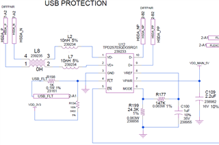
Based on the above design, in a working circuit, Vmode =. 5V and Vref = 3.5V,

In a malfunction circuit, Vmode .64V and Vref = 4.57V.

Can you provide your expert advice on what would cause Vref to jump to 4.57V?

Thank you,

Tony

  • Hi Tony,

    Can you please provide the gerbers for review of the PCB layout, as well?

    BR,

    Seong

  • Hi Seong,

    Here's the USB path layout, connector to MPU, 2 layers, top and bottom, 90~102 Ohm.

    Thanks,

    Tony

  • Hi Tony,

    Are you hiding any inner layers from image provided, or are you saying your PCB is 2 layers only?

    If it is 2 layers only, this is what is causing the issue. With DC, the return current takes the way back with the lowest resistance. At higher frequencies (starting from around 20kHz), the return current flows along the lowest impedance path, this lowest impedance path is usually the reference plane adjacent to the signal (a solid GND plane). High-speed USB 2.0 is 480Mbps, which translates to about 240MHz.

    For this reason it is always best to have a solid ground plane (or power plane) on the layer below. This return path helps to reduce impedance changes.

    BR,

    Seong

  • Hi Seong,
    It’s a 4-layers board. Transmission lines are referenced to the 2 inner layers, GND and Power.
    Gerbers attached.
    Thanks,
    Tony

    CAM.zip

  • Hello Tony,

    Thank you for providing the gerbers. I reviewed them and the following is my feedback:

    1. The recommended cap value for VPWR is 10uF. The schematic shows C109 is a 2.2uF. 

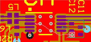
    2. The image below is of U2 (TPD2S703QDGSRQ1) on the TPD2S703Q1EVM. I've highlighted the VPWR and VREF caps in green. Also highlighted in pink is the ground via next to these caps and the IC's ground pin connected to the top layer ground plane with 6 ground vias. 

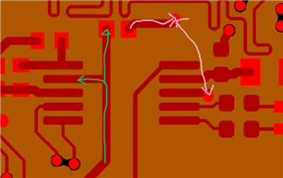
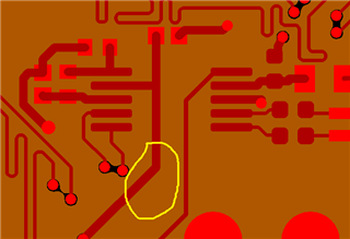
    The image below is from the gerbers you shared. The first difference versus the EVM is although the VPWR and VREF bypass caps are placed close to the device pins, they are not connected to a solid ground. Attaching them to a solid ground minimizes voltage disturbances during transient events. Second, the C109 decoupling cap's path to ground is along a short trace, which reduces it's effectiveness to filter noise; you always want to ensure a direct path to ground to minimize parasitic inductance. Third, the placement of the decoupling cap, although not far from the VPWR pin, comes after it. You want all noise to see the decoupling cap first before anything else so that the IC is powered via energy from the capacitor rather than directly from the voltage rail. 


    Do you suspect that there is reasonable amount of noise in the VDD_MAIN_5V voltage rail and current spikes in the system ground plane? The first thing I would try on your current board design is using a higher capacitor value for C109; perhaps even higher than 10uF. And/or making a modification and adding a decoupling cap where circled in yellow in the image below.

    Considering that the Vmode and Vref voltages are skewed on the failing boards versus working, I would say the culprit is transient events, such as ESD, may have damaged the ICs on the non-working boards. Transient events can be protected by improving the PCB design. 

    BR,

    Seong