- Ask a related questionWhat is a related question?A related question is a question created from another question. When the related question is created, it will be automatically linked to the original question.

Original question:

Tool/software:
Dear Receiver,
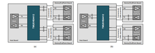
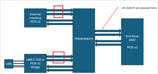
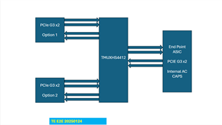
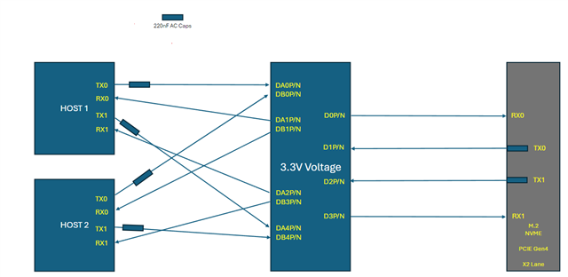
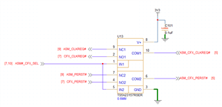
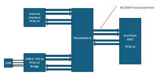
We have a setup as shown below
Kindly help me answering below queries.
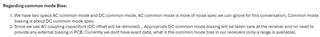
01. Is the AC cap placement correct?
02. The impedance 85Ohms supported for all the ports?
Kindly request you to write back as soon as possible. we are moving to Tape out phase soon.
Regards,
Sayeed Khan