This thread has been locked.

If you have a related question, please click the "Ask a related question" button in the top right corner. The newly created question will be automatically linked to this question.

TCAN4550-Q1: Delays Observed in CAN message transfer

Part Number: TCAN4550-Q1
Other Parts Discussed in Thread: TCAN4550,

Tool/software:

Dear Team,

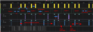
We are using TCAN4550 with the iMX8DXL processor connected using SPI. While we perform CAN message transfer, we are observing a few delays, due to which the throughput is also reduced. Detailed information and our few queries are added in the attached document. Do let me know if you need any extra information.

/cfs-file/__key/communityserver-discussions-components-files/138/Issue-Observed_5F00_TI.pdf

Regards,

Ankita

  • Hello Ankita,

    The processor controls the SPI timing and is responsible for all of the delays you have identified.  The TCAN4550-Q1 will accept data on the SDI pin and output data on the SDO pin solely based on the SCLK edge transition.  The nCS, SCLK, and SDI signals are generated by the processor and therefore there is nothing in the TCAN4550 that can help optimize or adjust those delays you have identified.

    The TCAN4550-Q1 datasheet provides the switching characteristics for the TCAN4550-Q1 interface.

    In terms of SPI optimization of the TCAN4550-Q1 throughput, the only recommendations I have are:

    - Increasing the SPI clock frequency to the maximum level that is supported

    - Using the Length field to allow multiple consecutive registers or MRAM data cells to be read/written in a single SPI transaction instead of single 32-bit word transactions.  This reduces the overhead SPI bits that come from the 32-bit header word (R/W Op Code, Address, and Length field) at the beginning of each SPI transaction.  This also reduces the idle time between the nCS pin transitioning High to Low between words.

    - Reducing the number register read/write transactions to a minimum.

    The overall CAN message throughput may depend on the processor load and how efficient it is with handling the SPI communication with the TCAN4550-Q1.

    Regards,

    Jonathan

  • Hi Jonathan,

    Thank you for the reply. We wanted to know about the below queries:

    • What is your test setup while checking this TCAN chip?
    • What about the delays involved? DId you find anything like these and can you provide the similar timing diagram? 
    • What was the throughput you have seen for 8byte and 64byte message for 1Mb and 5Mb data bitrates? 

    Regards,

    Ankita

  • Hi Jonathan,

    Additionally, after 26 messages (watermark) are received, an interrupt occurs, and before we see the actual data in SPI lines—that is, before cycle 1 as shown in the document's image—there are around six times as many CS toggles and some data is seen in the SPI lines. So, we wanted to know what these data's are.

    Regards,

    Ankita

  • Hi Ankita,

    What is your test setup while checking this TCAN chip?

    The TCAN4550 has been used and tested with many different MCUs and SPI protocol test equipment.

    What about the delays involved? DId you find anything like these and can you provide the similar timing diagram? 

    The MCU controls the SPI timing, and the TCAN4550-Q1 will simply receive or provide a data bit on the respective SDI and SDO pins for every SCLK cycle while the nCS pin is Low.  The delays associated with the SPI communication are from the MCU and this will vary between different MCUs, SPI driver firmware, and overall loading in the MCU etc.

    Yes, some MCU specific delays are common.  Some MCUs can process SPI transactions in full 32-bit or 64-bit chunks, while others can only support 16-bit or 8-bit chunks resulting additional delays in the SPI signals.  Other delays come from the overall load and what other functions the MCU is trying to support during the SPI communication.

    I can support you with any questions related to the TCAN4550-Q1 SPI timing in this forum.  If there are questions related to the setup/hold parameters listed in the specification tables in the datasheet, please let me know. 

    Any processor related timing delay questions are outside of the scope of this forum and I can only offer support at a general level as it pertains to the direct operation of the TCAN4550-Q1 device.

    What was the throughput you have seen for 8byte and 64byte message for 1Mb and 5Mb data bitrates? 

    Again, I don't have a specific number for you and this may vary due to a number of factors such as the ratio of the number of messages transmitted vs. received, the overall efficiency of the MCU SPI communication, and whether the MCU has to do any processing of the data between messages.  These are all application specific questions that you will need to determine.

    I can provide a simple spreadsheet tool that can be used to help calculate answers for these types of questions.  However, note that this spreadsheet assumes that a single 32-bit word is used for all SPI register and MRAM transfers.  This means that the Length field = 1 in every SPI header, and that for every 32-bit word of data, there is an associated 32-bit header word that contains the SPI read/write op-code, the Address, and Length field.  This doesn't include any efficiency optimization that comes from the burst mode type data transfers when multiple 32-bit words of data can be transferred in a single SPI message when the Length field is set to a larger number.  Doing so would reduce the number of Header words required and improve the overall efficiency of the SPI communication.  If your application is taking advantage of the Length field burst-mode communication, then you will need to factor that into your calculations.

    3125.Throughput Calculator v1.xlsx

    Additionally, after 26 messages (watermark) are received, an interrupt occurs, and before we see the actual data in SPI lines—that is, before cycle 1 as shown in the document's image—there are around six times as many CS toggles and some data is seen in the SPI lines. So, we wanted to know what these data's are.

    The image in your document doesn't show what the MOSI and MISO data bytes are, so I would suggest you zoom into your logic analyzer capture to determine exactly what the data being transferred is.  I suspect it is related to reading and clearing the interrupt register bits, reading the RX FIFO Status register to get the RX buffer Get Index, etc.

    Regards,

    Jonathan

  • Hi,

    Thank you for the reply.

    We wanted to know that in the Software User's Guide Section 5.2, it was mentioned as, "The TCAN45xx SPI header has a word parameter, which tells it how many words (4 bytes each) of data will be transferred." So is it possible to increase it to 8 bytes in the default 5.15 tcan4x5x driver code? If so, do let us know, or if there is any patch that you can provide, it will be great.

    Regards,

    Ankita

  • Ankita,

    The multi-word write and read functions are already included and this is being referred to as "burst" mode communication. Please see the TCAN4x5x_SPI.c file for the functions. 

    There are 3 functions associated with a burst write or read SPI transaction because this requires some special handling of the chip select (nCS) signal that must remain Low for the entire length of the SPI transaction.

    The first "start" function pulls the nCS pin low and writes out the Start Address and the number of 32-bit words of data that are going to be transferred in this transaction.

    The second burst "write" or "read" function transfers the data.

    The "end" function pulls the nCS pin high again at the end of the SPI transaction.

    Regards,

    Jonathan

  • Hi,

    Does this TCAN4x5x_SPI.c present in the default 5.15 BSP? Does this file need to be added? If so, do share the file.

    Regards,

    Ankita

  • Hi Ankita,

    I'm sorry, I thought you were referencing our TCAN4550 Demo Software reference code (Link), but it appears you are referencing the Linux driver.

    I'm not a Linux expert and I support the TCAN4550 at the device level, but I believe the originally released driver only used single word SPI transactions.  There was a revised driver released in 2023 to optimize the throughput of the driver as best as possible using multi-word SPI transactions.  I'm not sure which version you are using, but the latest released driver is the best driver available.

    Regards,

    Jonathan

  • Hi,

    Thank you for the reply. We are using 5.15.52 version of BSP. Can you send us the link for this latest released updated driver code?

    Regards,

    Ankita

  • Hi Ankita,

    Again my expertise with with the TCAN4550 device and not with Linux.  I know the updated driver was upstreamed into the Linux Kernel in 2023 and is now supported by the Linux community and can probably be found through normal Linux code repositories.  But because I don't use the TCAN4550 through Linux, I don't have any specific links or information about the driver itself.

    If you have any questions related to the configuration of the device registers or operation, I am more than happy to help you with those.  But I'm not a good resource for Linux related questions and you can probably get better answers through forums that are dedicated to Linux related questions.

    Regards,

    Jonathan

  • Hi,

    Thank you for the reply. We wanted to know that on the TCAN side do you restrict to use only GPIO based chip select line? or can we make use of native chip select. Because on using the native chip select  we get kernel panic while initializing the tcan module. It would be great if you could get information regarding this.

    Regards,

    Ankita

  • Hi Ankita,

    The SPI Chip Select is an input signal to the TCAN4550 and it only has a few requirements, none of which are related to how the processor controls this signal.

    The TCAN4550 requires:

    • The Chip Select signal transition low at the beginning of every SPI read/write transaction (it can't be permanently tied low).
    • The Chip Select signal must remain low for the entire duration of the SPI transaction which consists of at least 64-bits (and clock cycles).
      • The first 32-bits are from the Header word that contains the read/write op-code of 0x41 or 0x61, the address of the register or MRAM location, and the number (or length) of the data to read/write from the address location.
      • There are an additional 32-bits for each data word as indicated in the Length field of the header word.
    • The Chip Select signal must transition high at the end of every SPI read/write transaction
    • The number of clock cycles that were detected while the Chip Select was low must be a multiple of 32, and match the number of clock cycles needed for the header + data words as indicated by the Length field.  (64-bits for Length = 1, 96-bits for Length = 2, etc.)

    The native SPI peripheral drivers may vary between processors, and many processors are unable to work with full 32-bit words, or multiple 32-bit words and want to drive the chip select low and high after each 8, 16, or 32 bits of data which will cause an error.  Therefore, GPIO control of the chip select may be needed.  However, if the processor's native driver can be configured to hold the chip select low for the correct number of data bits to meet the TCAN4550's requirements, then this would be ideal.

    But from the TCAN side, as long as the chip select and corresponding SPI data/clock signals meet the timing and format requirements outlined in the datasheet, it doesn't care how the processor controls the chip select signal and whether it is from the native driver or through GPIO control.

    Regards,

    Jonathan

  • Hi Jonathan,

    Thank you for the reply. Now we have configured the native chip select in default 5.15 BSP, and we could initialize the tcan module and make the can link up, but with this we are not being able to do any message transactions. So any idea that can help us in solving this issue?

    Regards,

    Ankita

  • Hi Ankita,

    If I understand you correctly, you are able to communicate with the TCAN4550 through SPI, bu you are not able to send or receive any CAN messages.  Is that correct?  I'm not exactly sure what it means to "make the can link up."

    If so, can you do a readout and create a log file of the TCAN4550 registers with the final value after the configuration is complete?  I could review the final device configuration for errors.

    Monitoring the Status, Interrupt, Error Counter, and Protocol Status registers can also provide information on error conditions when trying to send or receive CAN messages that might help identify the problem as well.

    Regards,

    Jonathan

  • Hi Jonathan,

    Thank you for the reply. Above one worked and we have few additional queries 

    Here, cycles 4 and 5 have the actual data that we have sent, and in those last 4 bytes are the actual data. Also, before this actual data cycle, there are 3 extra cycles that we have observed in each 8-byte data tarser. So we wanted to know if these total 6 cycles are expected in the SPI based CANFD transmission and also what are those? And also in Cycel 4 and 5, apart from actual 4 byte (32 bit) data, there is another 4 byte of data, so what are these, and can we make this to transfer for 8 byte together so that the two cycles reduce to 1 cycle of actua transfer?

    For detailed info on the data in the cycle, I have attached the LA session in the mail since I was not able to attach it in the forum.

    Regards,

    Ankita

  • Hi Ankita,

    I haven't seen an email with the LA session.  I'll send an email to see if we can connect and use that for sharing the LA session data.

    Regards,

    Jonathan